Assembling the PHCC Motherboard (Rev.4B)
Intro
The Motherboard is the central part of the PHCC system. On one side, it connects to the PC and talks to your application program, and on the other side it manages all the inputs and outputs. The DOA, DOB, keymatrix,... daughterboards all connect to the motherboard.
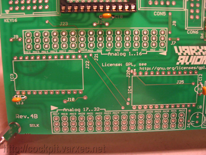
Directly onboard it has 33 channels of analog inputs, the serial port, and a connector for the optional USB daughterboard.
It requires a powersupply that outputs regulated +5V DC. There are two ways to hook up the supply voltage to the motherboard,
- via CON2, a floppy power connector
- or via CON1, a simple two-pin header
It is recommeded to use a PC (AT or ATX) power supply. It is also recommeded to hook up power via CON2. Since the other one, CON1, does not provide protection against reversed polarity.
Assembly
First start with the smaller components and work your way up to the bigger ones like sockets and connectors. This helps at places where the bigger stuff might get in the way of soldering smaller parts.
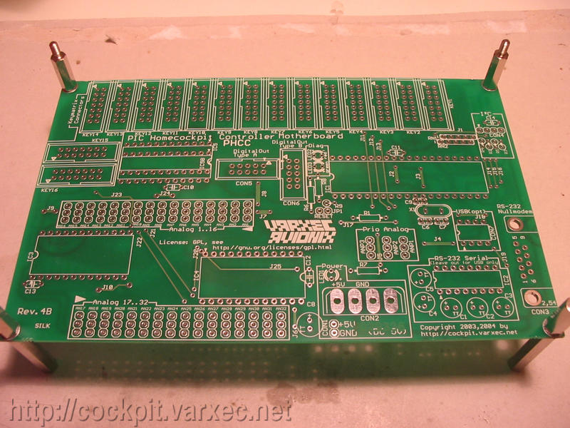 |
The bare Rev.4B motherboard. |
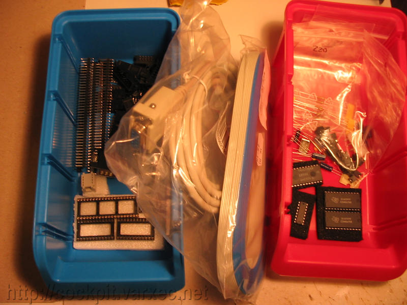 |
Overview over the parts of the full kit. (The red and blue plastic boxes are not included) |
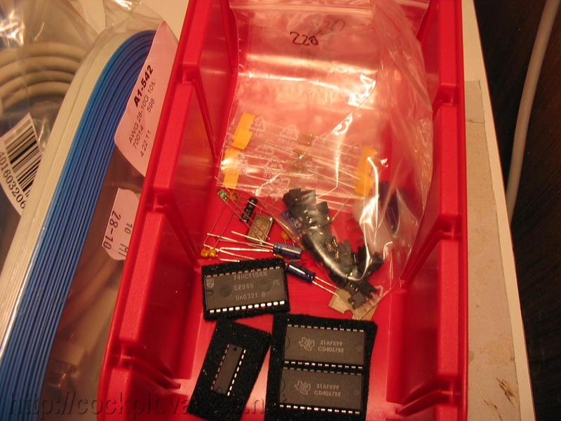 |
Here's whats in the red box. Mostly the smaller parts: resistors, capacitors, ICs, crystal oscillator,... |
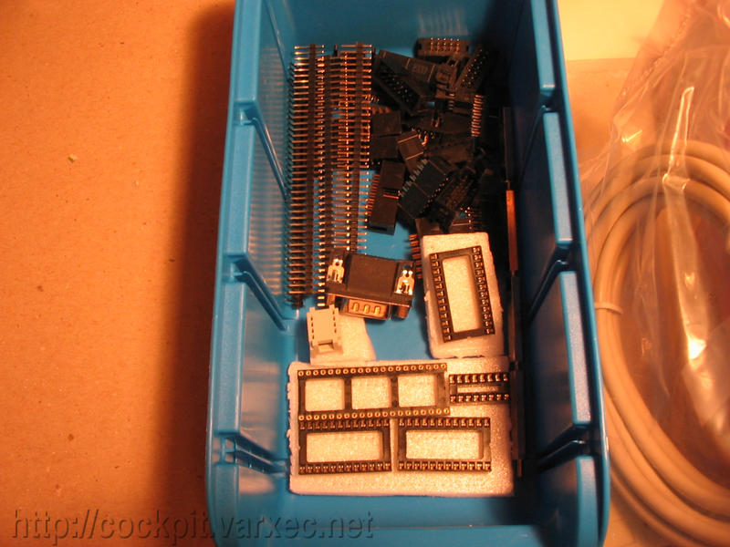 |
And the stuff in the blue box, mostly mechanical stuff: sockets and connectors |
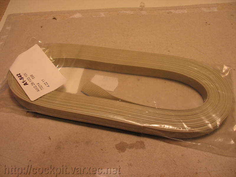 |
The cables: 10 meters of 10pin flat cable. Used for DOA and DOB connections. |
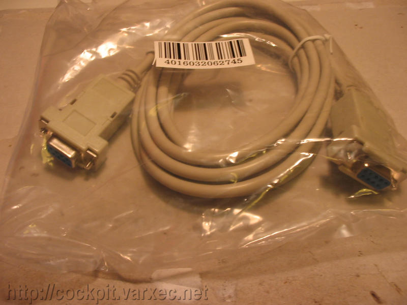 |
and the serial null-modem cable for the connection to the computer. |
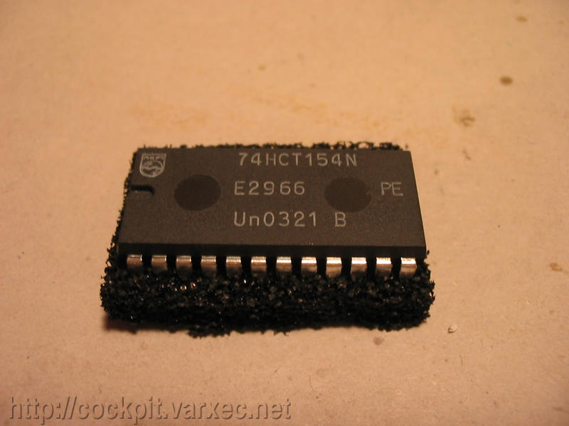 |
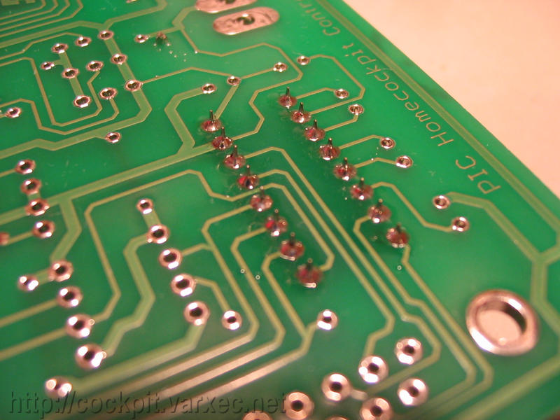
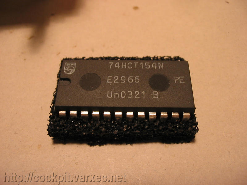
Now the parts in detail: a 74HCT154 1-of-16 selector. (IC5). |
|
This IC sometimes comes in a 300mil (-> half width) package. |
|
| The motherboard supports both types of packages (600mil and 300mil). | |
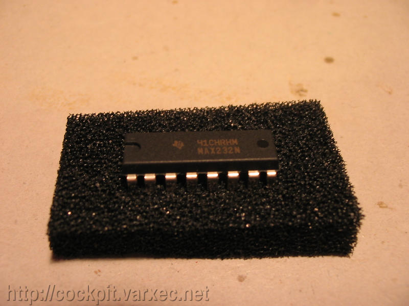 |
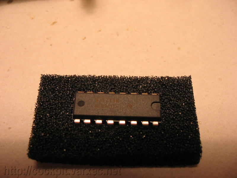
The MAX232 RS232 level converter. (IC2) |
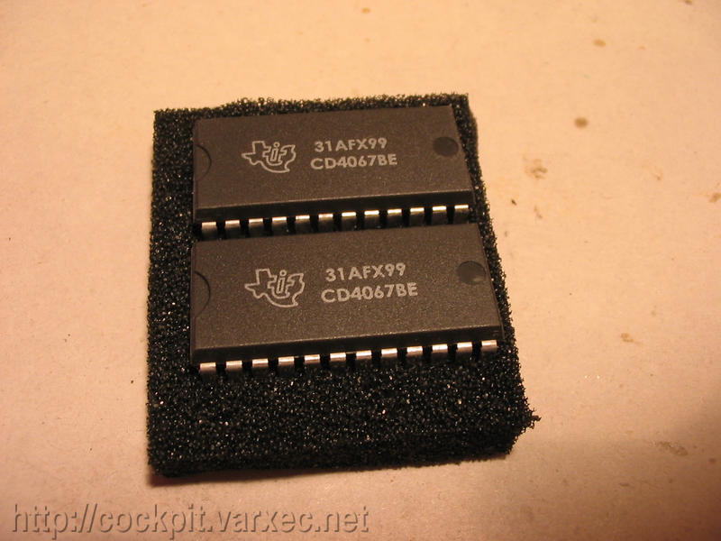 |
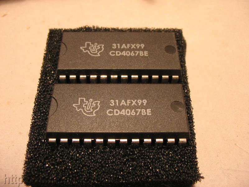
The CMOS 4067 analog multiplexers. (IC3/IC4) |
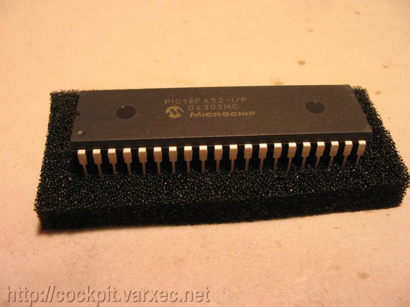 |
The "heart" of the system, a PIC18F452 microcontroller. (IC1) |
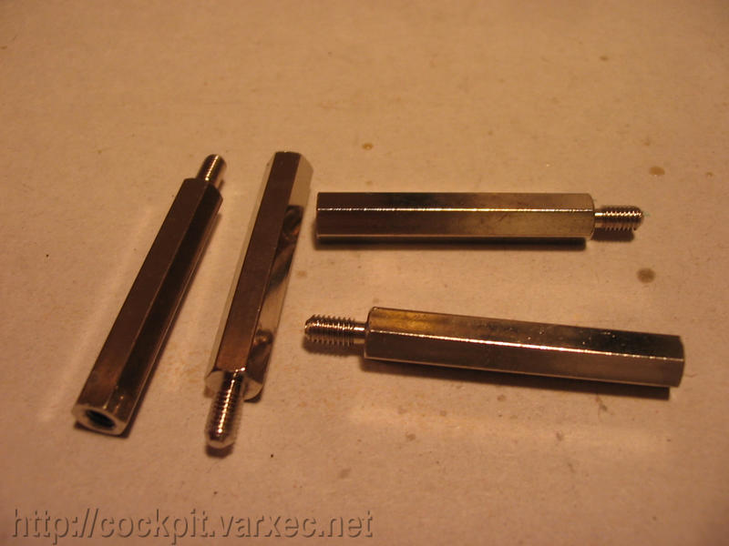 |
Four spacers for board stacking/mounting. They fit the 3mm holes in the four corners of the board. |
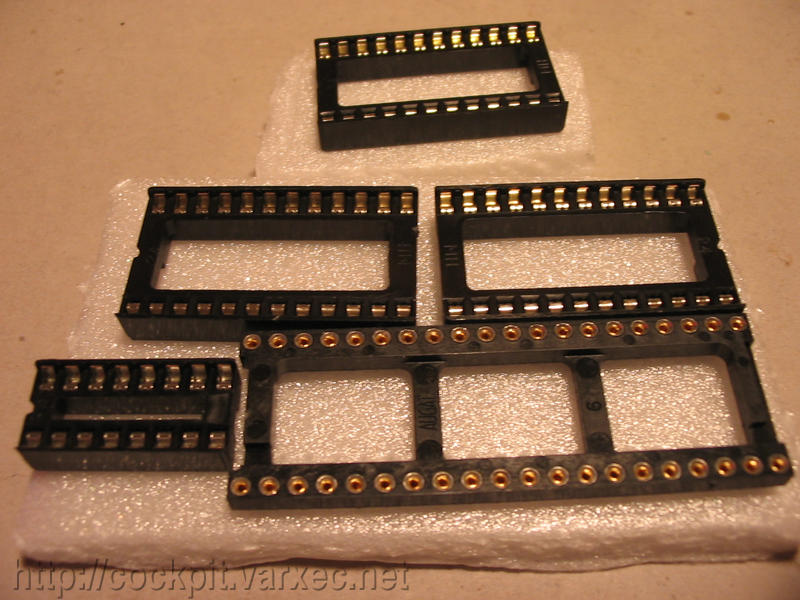 |
The sockets for IC1-IC5. The socket for the PIC (the biggest one) is a precision/turned type. |
 |
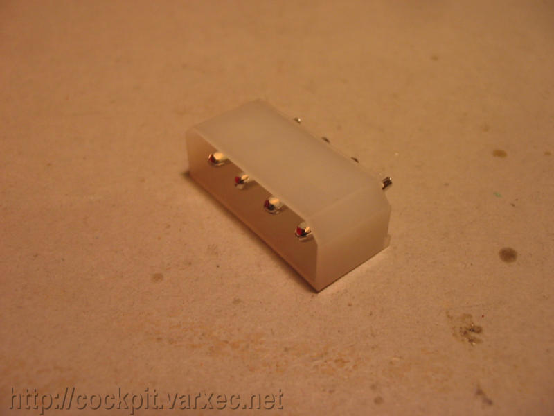
This is the connector for the USB daughterboard (CON7). The pins are in DIP8 format, and it takes an 8 wire flat cable. |
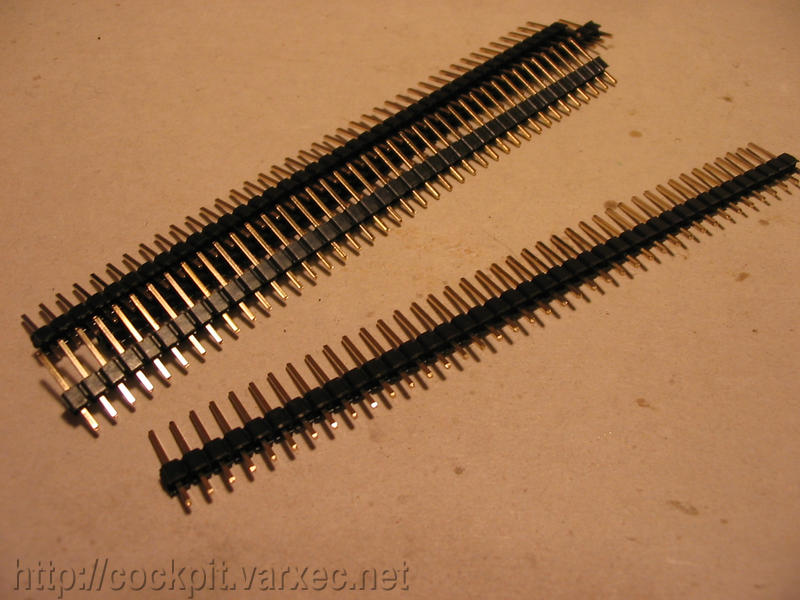 |
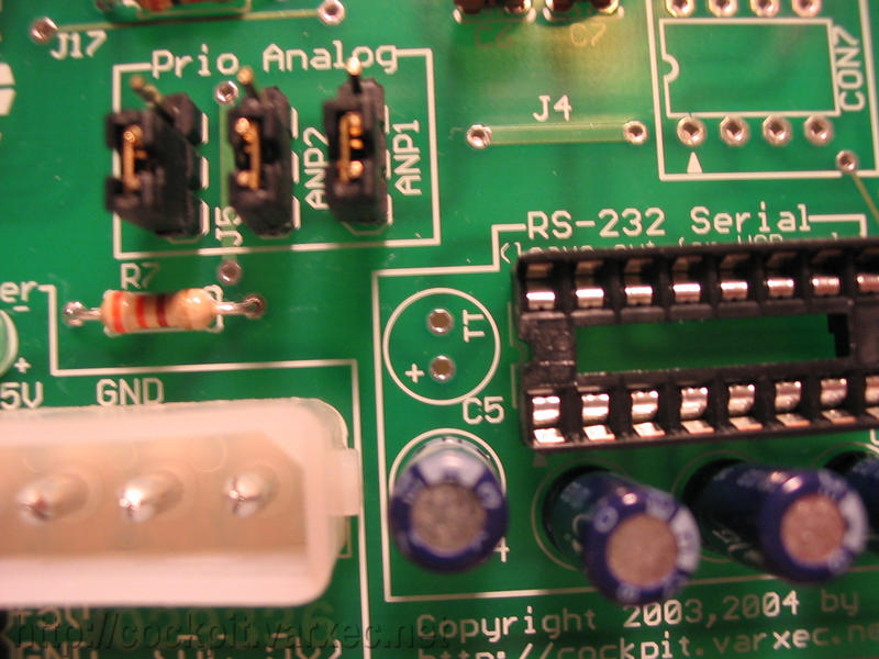
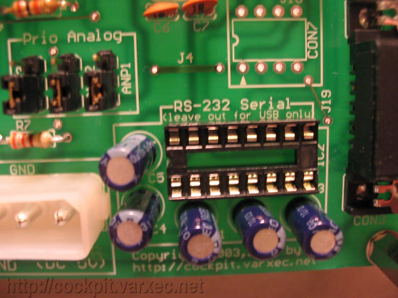
The pinheaders for power (CON1), I2C (CON4), reset (JP1), primary analog inputs (ANP1-3), secondary analog inputs (AN1-32). |
| These have to be broken down into the respective sizes. two for CON1,JP1; three for ANP1-3,AN1-32; and four for CON4. | |
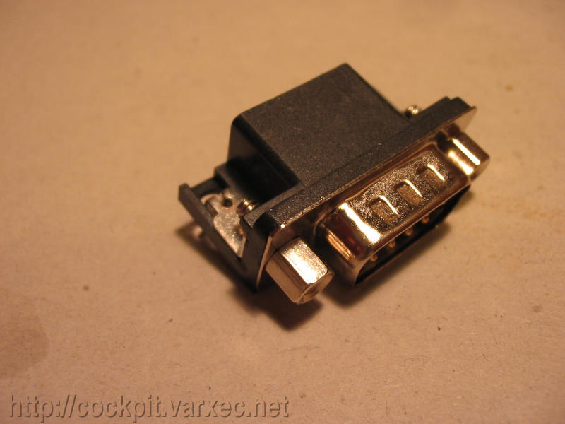 |
The serial port. (CON3) |
 |
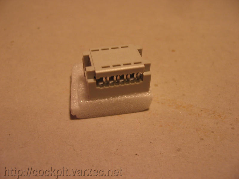
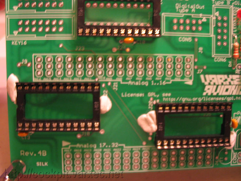
The keymatrix daughterboard connectors. (KEY1-16). They are shrouded IDC 14pin pinheaders. |
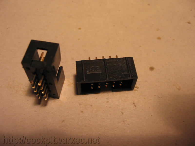 |
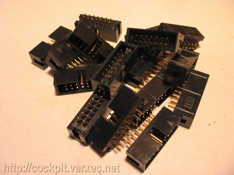
The DOA and DOB connectors. (CON5/CON6). They are shrouded IDC 10pin pinheaders. |
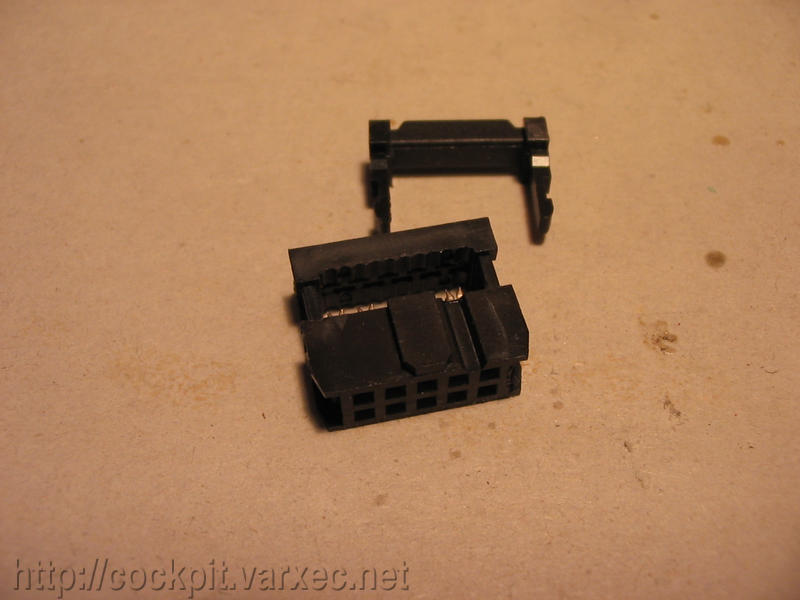 |
10pin IDC connectors for DOA and DOB. |
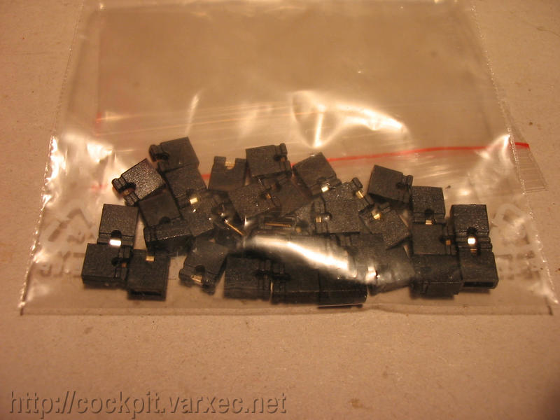 |
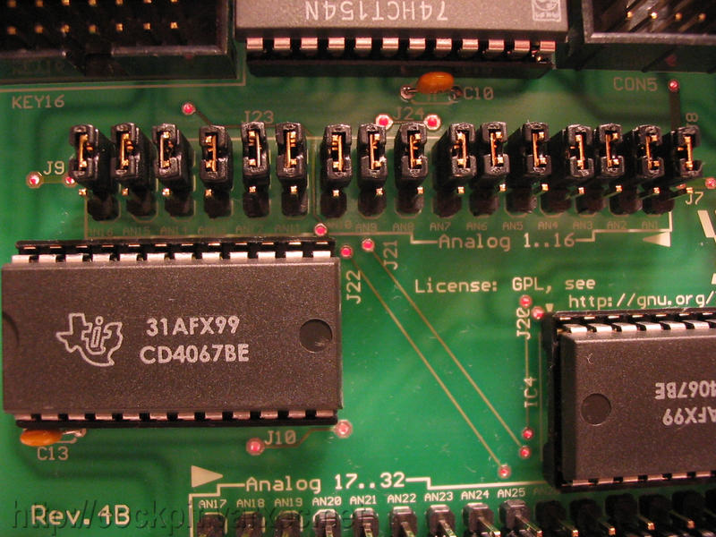
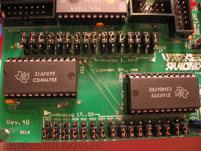
35 jumpers. These are used to short the analog inputs to +5V or GND. This keeps the unused inputs from floating. |
| Floating inputs mean constantly changing values. If the inputs are set to GND or +5V, they remain stable and thus reduce the amount of updates sent to the PC. | |
 |
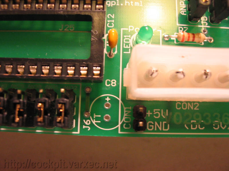
The floppy power connector. (CON2) |
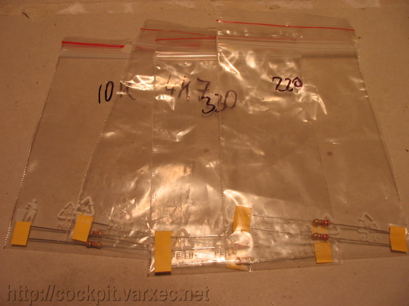 |
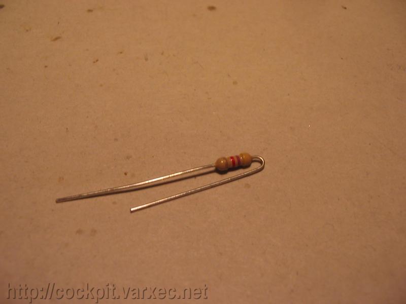
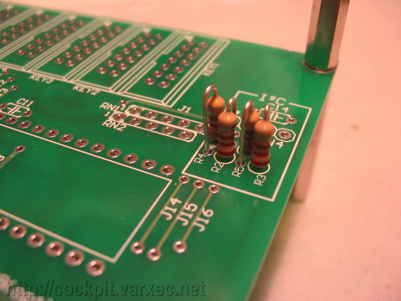
Four different values of resistors (9 resistors total). (R1-9). Values are: 220, 330, 4.7k, 10k. |
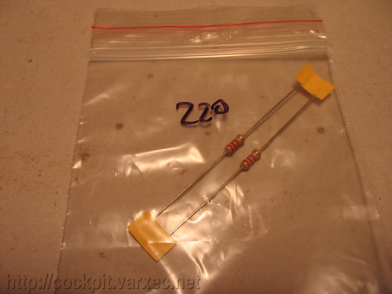 |
Two resistors, 220 Ohms. (R2/R3) |
 |
Three resistors, 330 Ohms. (R6-8) |
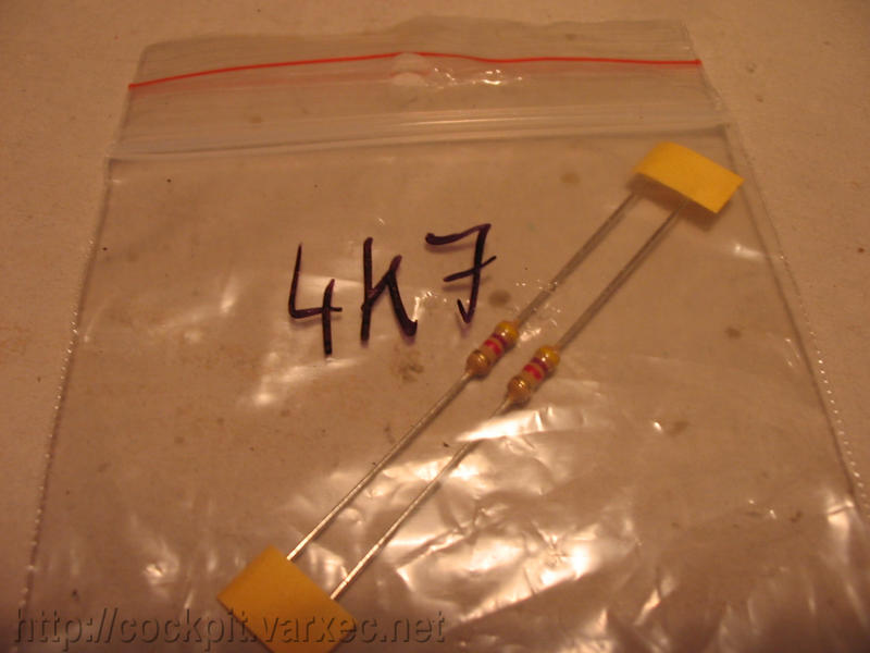 |
Two resistors, 4.7kilo Ohms. (R4/R5) |
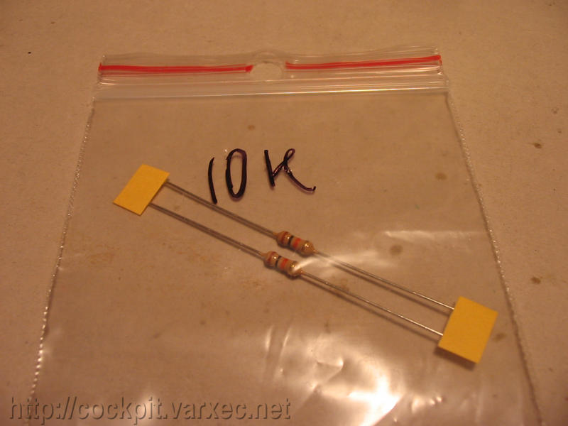 |
Two resitors, 10kilo Ohms. (R1/R9) |
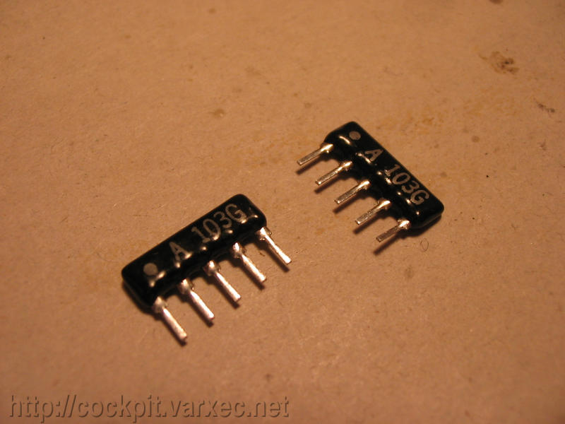 |
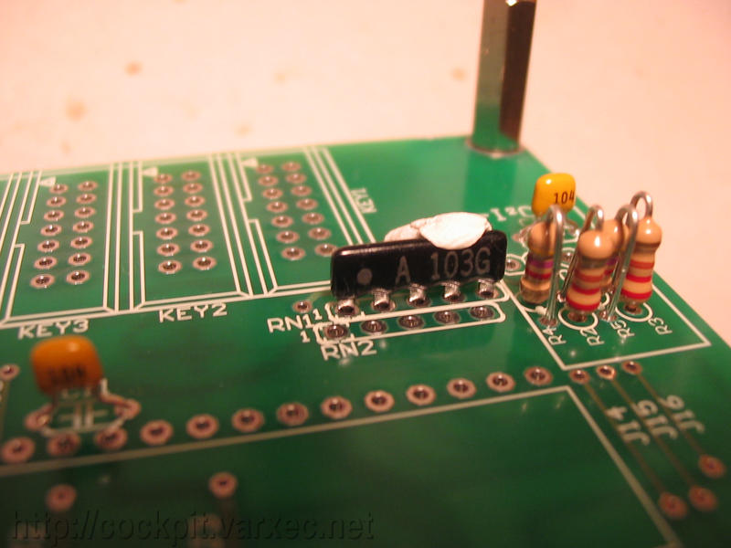
The pullup resitor-arrays. (RN1-2) |
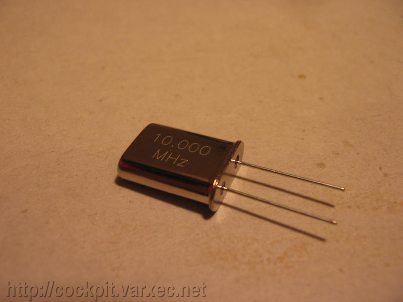 |
The crystal oscillator (quartz oscillator). (X1) |
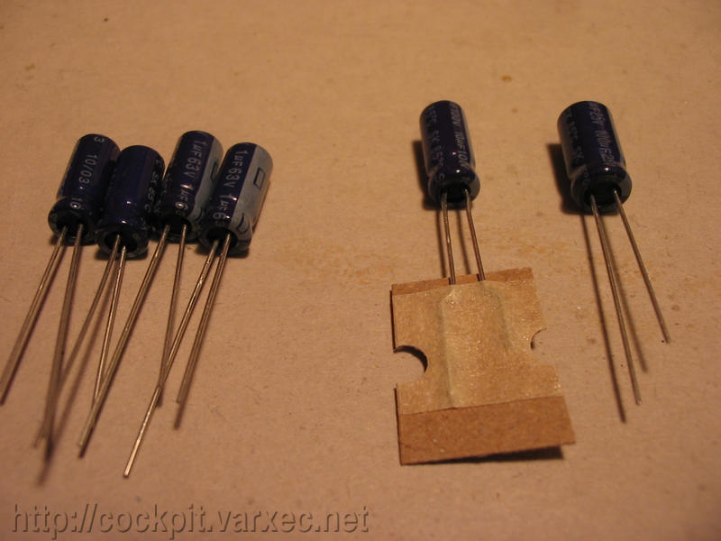 |
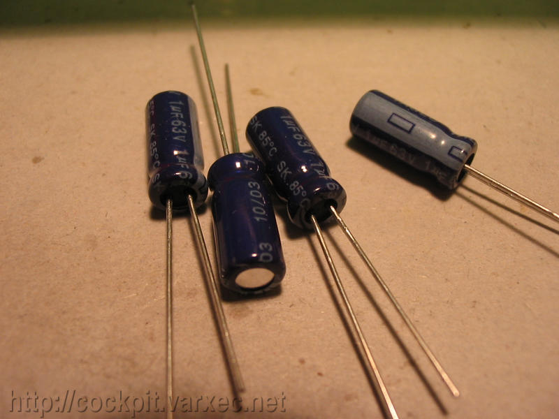
Six electrolytic capacitors in three values: |
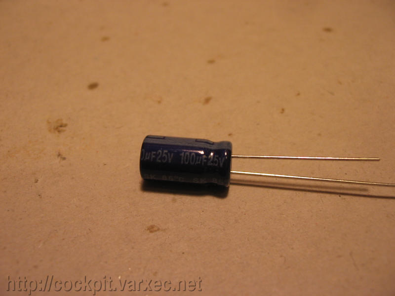 |
One with 100uF (micro farads), 25Volts rating. (C8) |
 |
Note: electrolytic capacitors are polarized (ie. they have a positive and negative terminal). Most types have the negative lead makred like this, with a "-" sign. Often, the leads have different lenghts. If this is the case, the shorter one is the negative lead. |
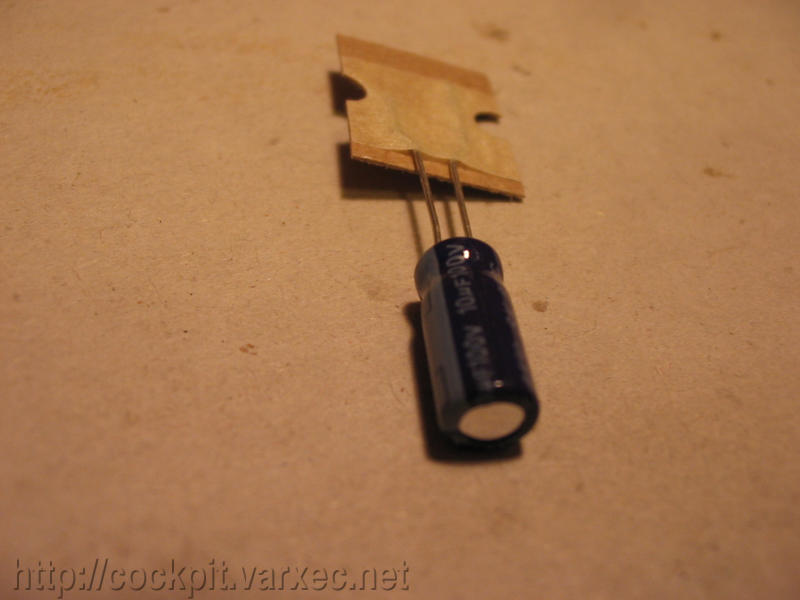 |
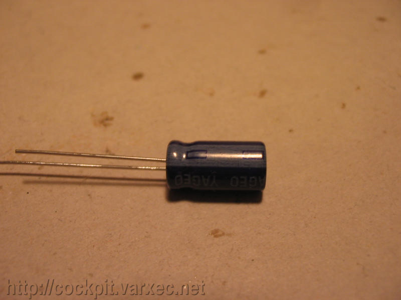
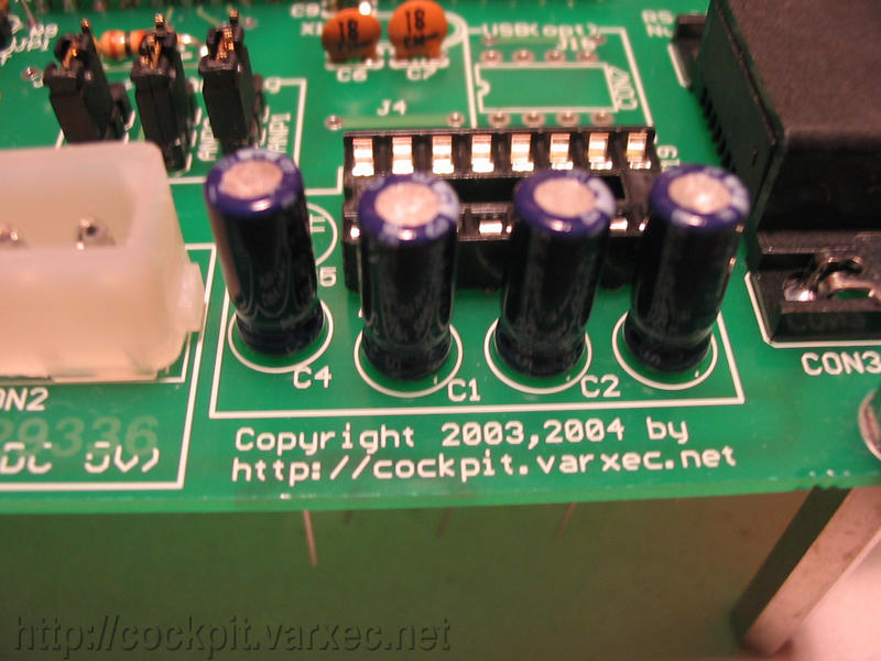
One capactitor with 10uF and 35-100V rating. (C5) |
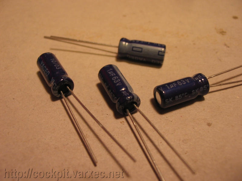 |
And four 1uF caps with a 35-63V rating. (C1-4) |
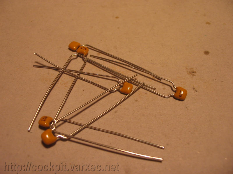 |
The other kind of capacitor used are ceramic caps with 100nF (nano farads). (C9-14). |
|
Ceramic capcitors are not polarized, so you can solder them in either way. |
|
|
These are used for the ICs and are placed close to the GND and Vcc lead of each IC. |
|
| These kinds of ceramic caps are often known by the type of dielectric they contain. X7R, Z5U, or NPO are common types. | |
 |
Additionally, two more ceramic capacitors. (C6/C7). These are the caps for the crystal oscillator. |
 |
Three LEDs, one to indicate power, and two for diagnosis/debugging. (LED1-3) |
 |
LEDs are polarized. When they are soldered in the wrong way, they won't do any harm, but they won't work either. |
| The short lead indicates the cathode (negative side). You can also check the "inside" of the LED body: the bigger metall part is always the cathode. | |
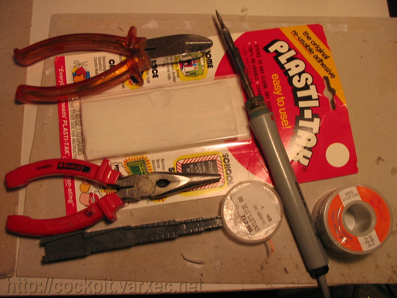 |
Not included in the kit, here are some tools needed or helpful to assemble the board. We'll go over them one by one: |
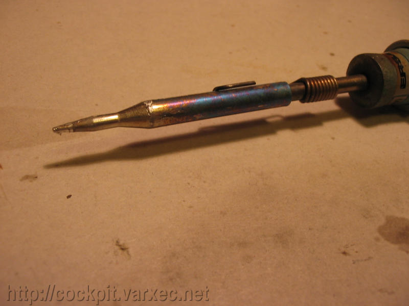 |
A soldering iron (or station). A fine tip will make the job much easier. The iron doesn't need to have a high watt-age. Mine has 16Watts. Higher watt-age means usually higher temperature (this does not apply directly to soldering stations). Stay under 30Watts for soldering irons. |
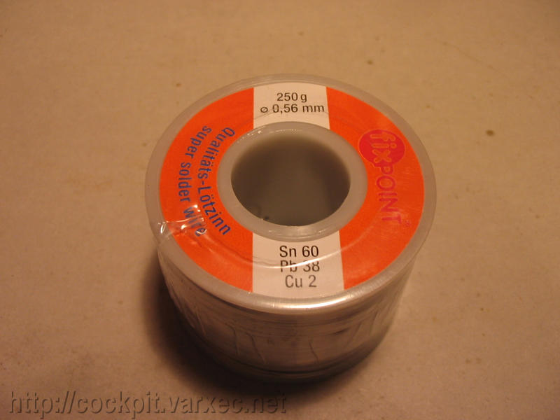 |
Fine solder wire. I'm using 0.5mm wire. The 1mm kind works too for the industrially made boards. If you made your board at home, you'll definately want to use the 0.5mm stuff. |
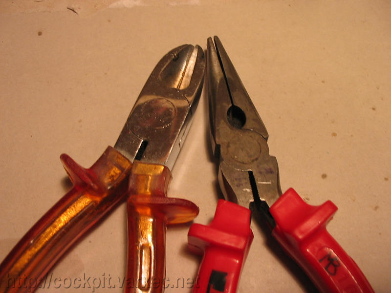 |
Pliers and wire cutters. |
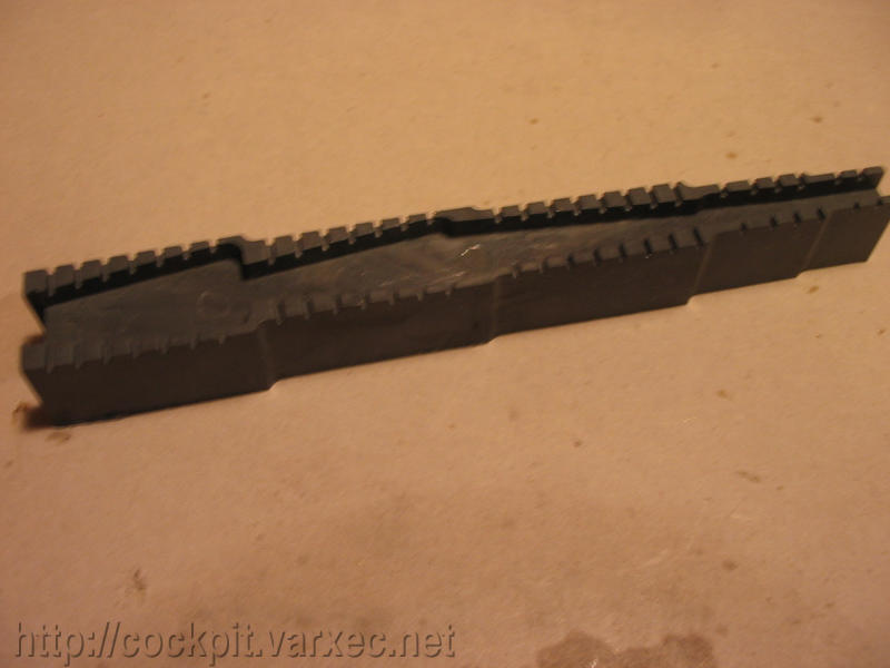 |
Nice to have but not necessary at all: a resistor/... bending helper tool. |
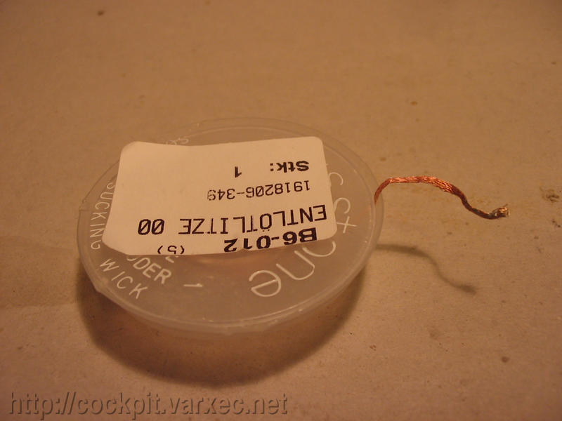 |
Helpful to fix areas with too much solder or solder bridges: solder wick. (copper braid with flux to suck up excess solder). |
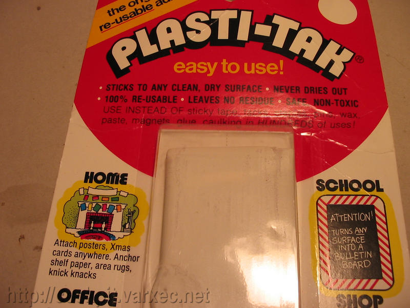 |
This is helpful when you want to "tack" parts in place for soldering. It keeps them from falling off the board when turned around for soldering. Its basically "adhesive removable putty". That stuff is sold under different names, eg Plasti-tak, sticky-tag,... |
 |
The back of the Plasti-Tak package with instructions. |
 |
This is how the stuff looks like. |
 |
Now .. on to the actual work. If you don't have a double-sided board, start off with the jumper wires, J1-J24. |
| As the board I have here is double-sided, I can skip this. | |
 |
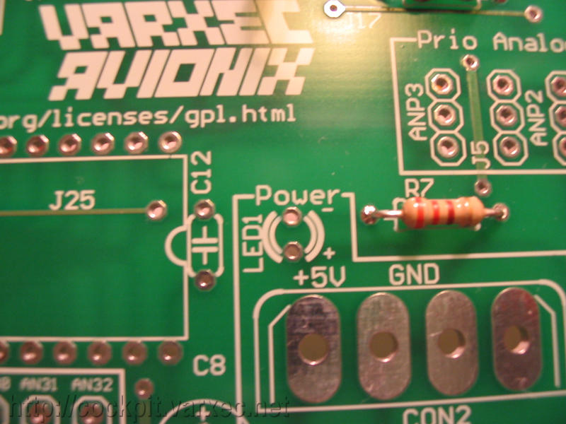
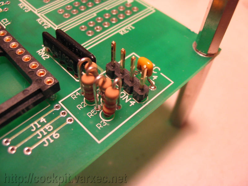
Starting with the resistors. First are the 330 Ohms resistors (color code: orange-orange-brown). First R7 ... |
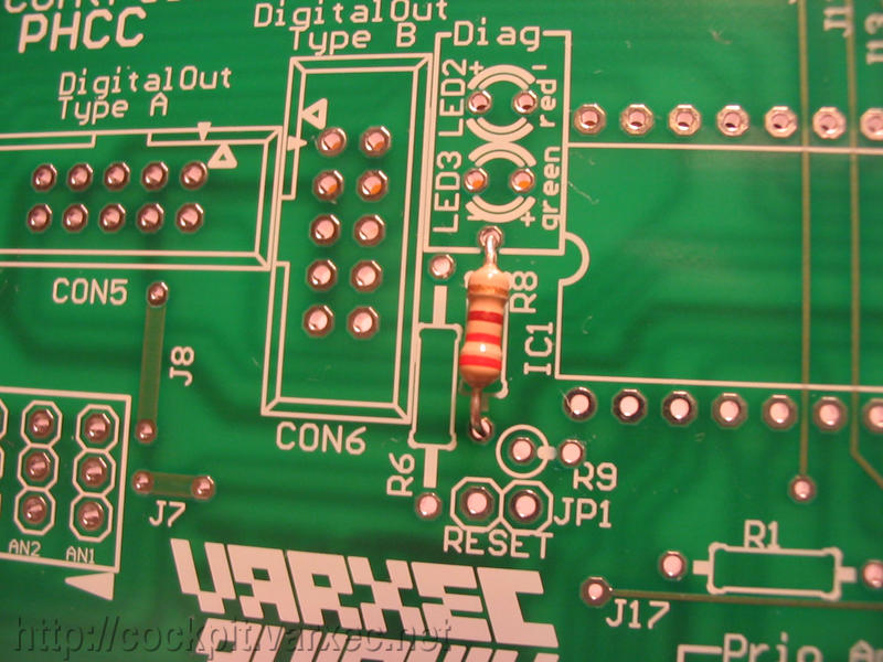 |
... then R8 ... |
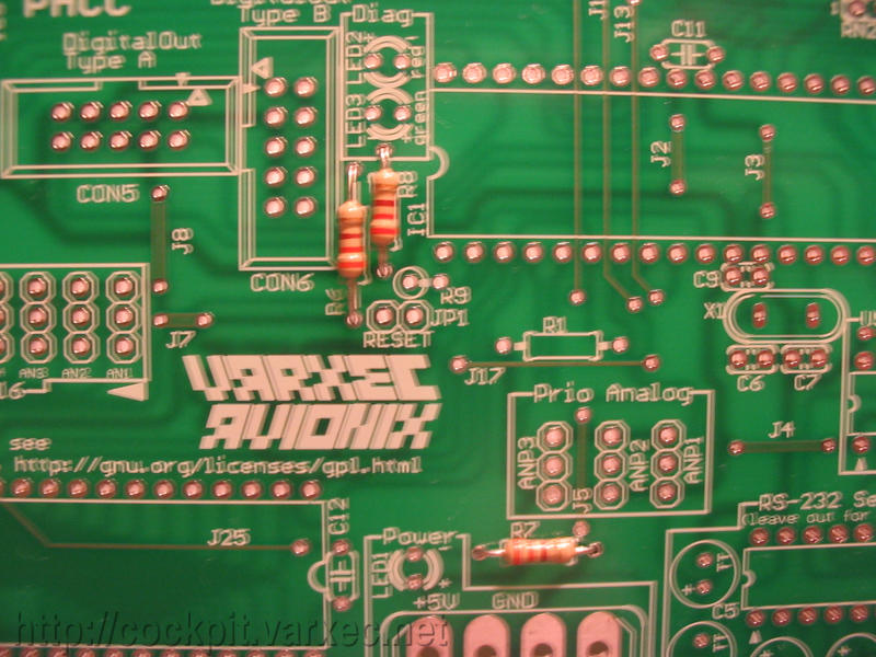 |
... and R6. |
 |
If you bend the leads on the underside outwards a little bit like shown, then the resistors can't fall out. |
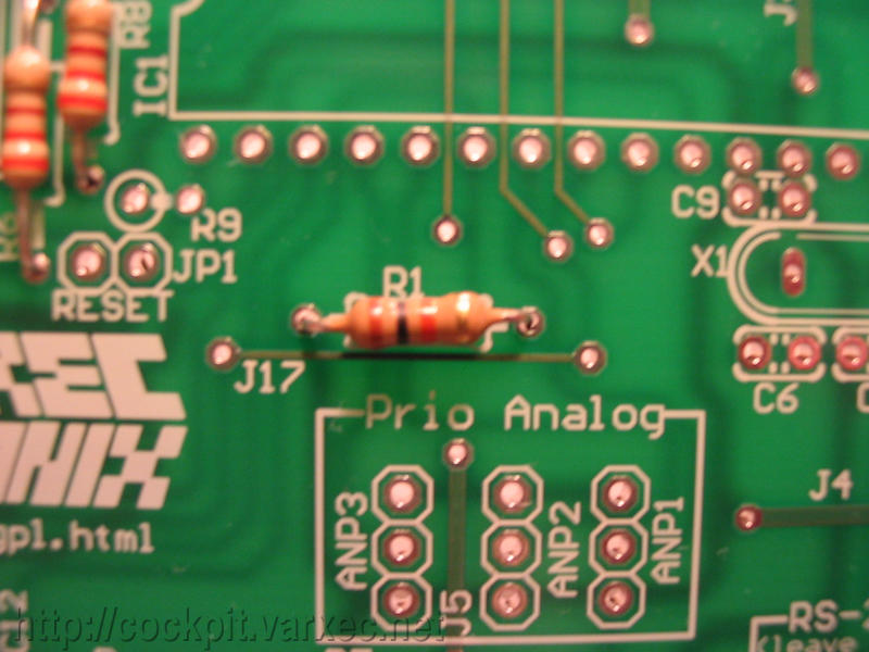 |
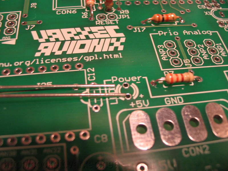
Next are the two 10k resistors (color code: brown-black-orange), R1 ... |
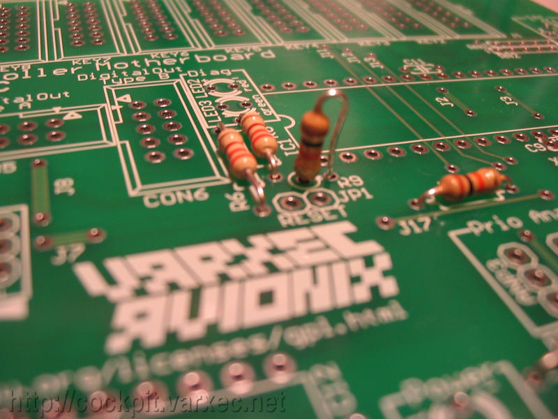 |
... and R9 (this one has to "stand up"). |
 |
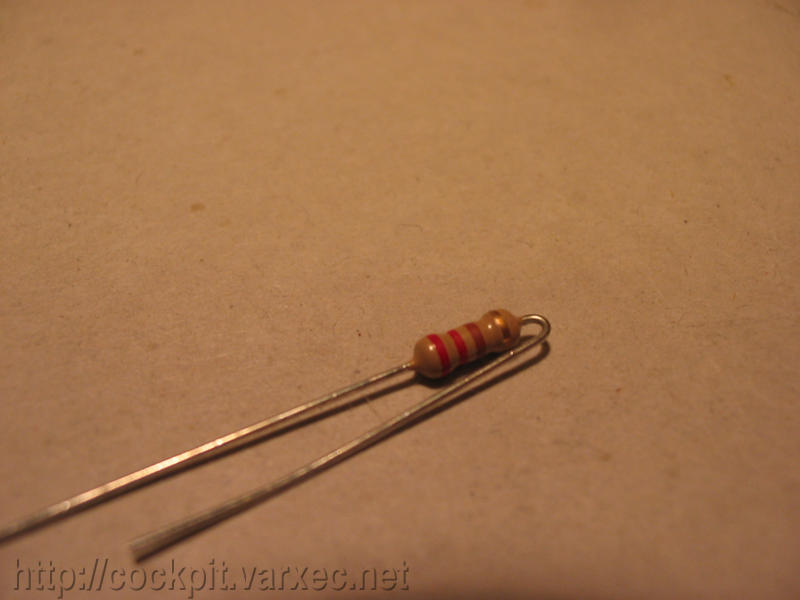
Now the 4.7k resistors R4 and R5 (color code: yellow-violet-red). They also have to keep standing. Bend one lead as shown... |
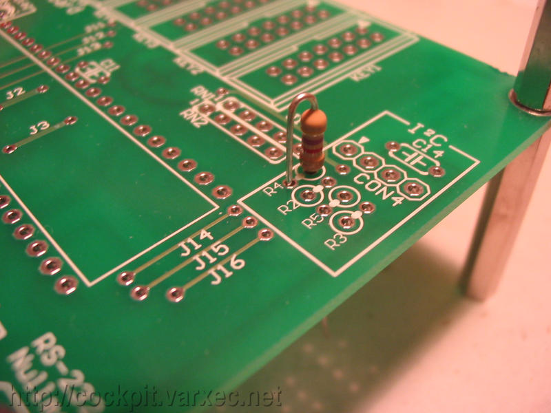 |
... and put the first into place... |
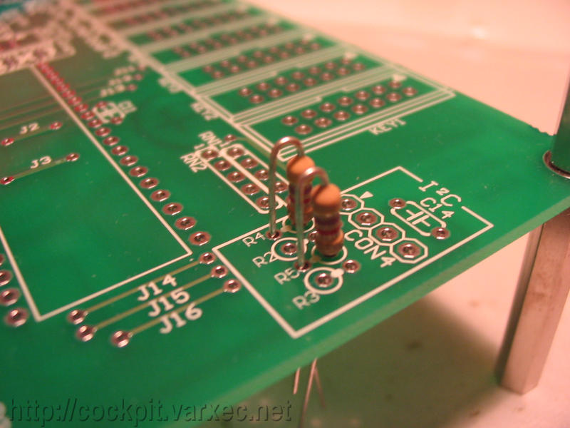 |
... and the second one. |
 |
Do the same with R2 and R3, the 220 ohms reeistors (color code: red-red-brown). |
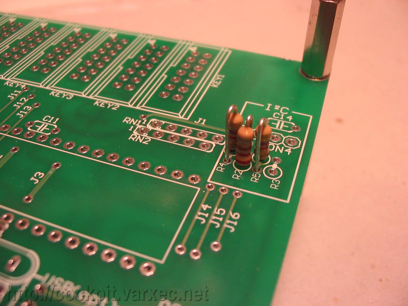 |
R2 ... |
 |
... and R3. |
 |
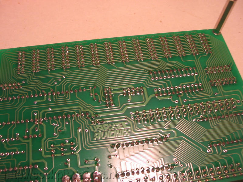
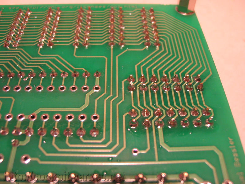
Turn the board over to the underside. Now solder all the resistors ... |
 |
... and after soldering ... |
 |
... all of them ... |
 |
... use a wire cutter to cut off the excess leads as shown. |
 |
Such as this. |
 |
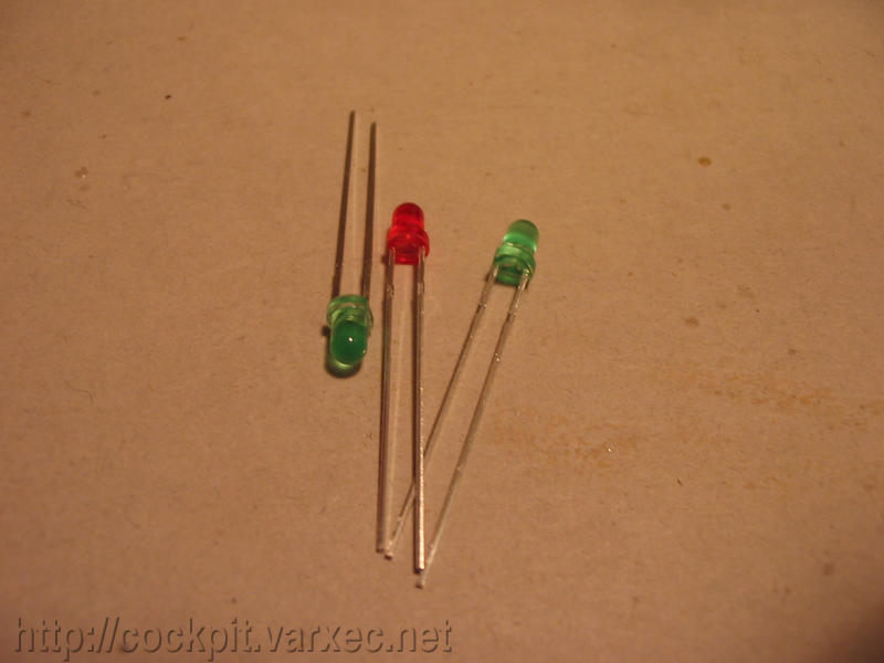
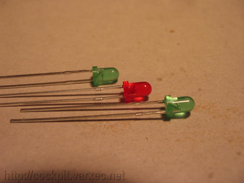
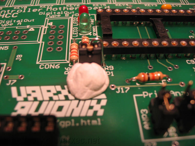
The next parts: the three LEDs. You can see here that the boards are marked with "+" and "-" next to the LED symbol. |
 |
The shorter lead of the LED is the cathode (negative side). This goes into the "-" hole. |
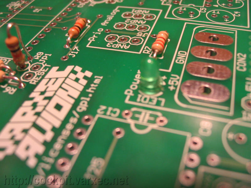 |
This was LED1. I use a green LED here. |
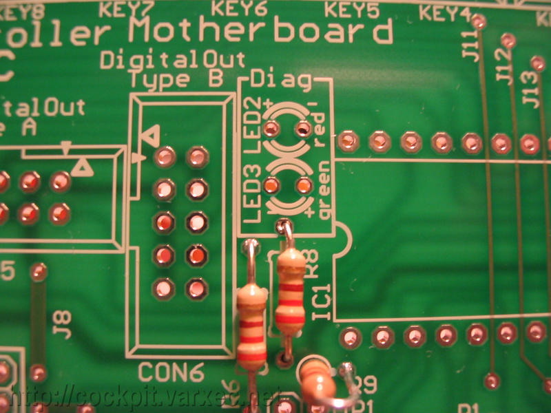 |
Now the Diag LEDs: LED2, LED3. I use a green one and a red one. Just note that the two LED's polarity are "reversed" |
| (ie. the "+" of the two LEDs are diagonally arranged... just look at the picture) | |
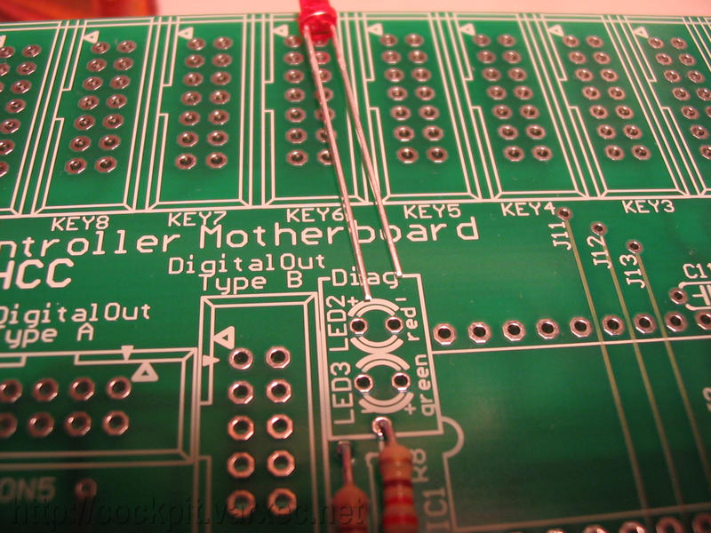 |
LED2, the red one. The cathode (shorter, negative lead) points to the right side. |
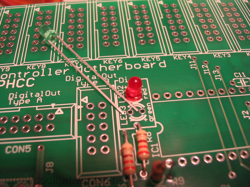 |
LED3, the (second) green one. The cathode this time points to the left side. |
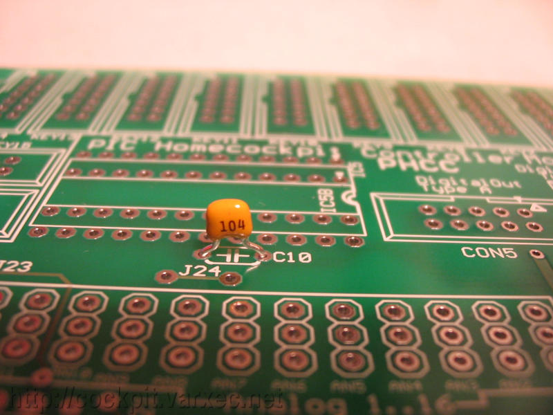 |
Moving on to the ceramic capacitors: C9-13. Those caps are not polarized, so they work in either direction. |
 |
One note about C9: This one has a different pitch (.1") than the others (.2"). I just used a .2" type and bent the leads so it fits the .1" spacing. |
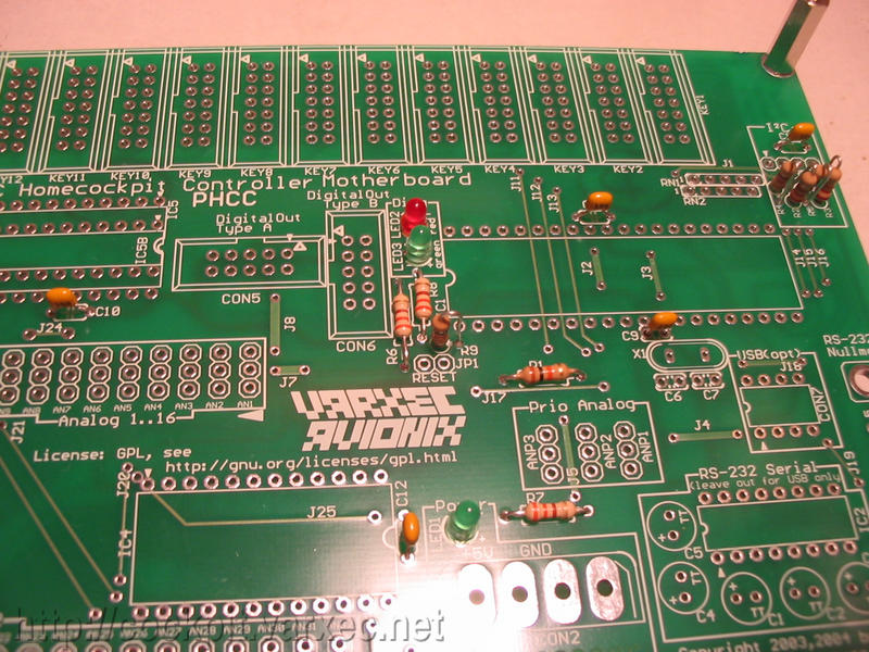 |
Our progress so far. |
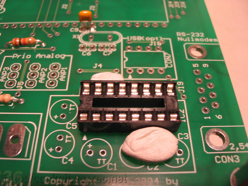 |
Now on the IC sockets. First the DIL16 socket for IC2. |
|
Note that one of the narrow sides is marked. It helps to align the IC correctly, pin 1 is where this mark is. For IC1, pin 1 is on the left side. |
|
| This is where the plasti-tak (removable adhesive putty) comes into play. I just use two blobs of it to fix the socket from two sides. It is enought to hold the socket in place. | |
 |
... until its soldered. |
 |
Next is the IC5 socket. Here you need to make sure you get the right type for the 74HCT154 package. As I already said, this IC is available in 300mil (the narrow inner one) and 600mil (the other wide one) width. I have a 600mil type. Pin 1 is on the right side. |
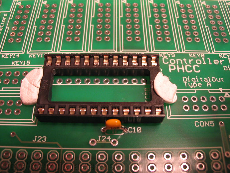 |
Fix in place with removable adhesive putty and solder. |
 |
The CMOS 4067 IC3 and IC4 sockets... (pin 1 of IC3 points is on the left, pin 1 of IC4 is on the right) |
 |
... same strategy here. |
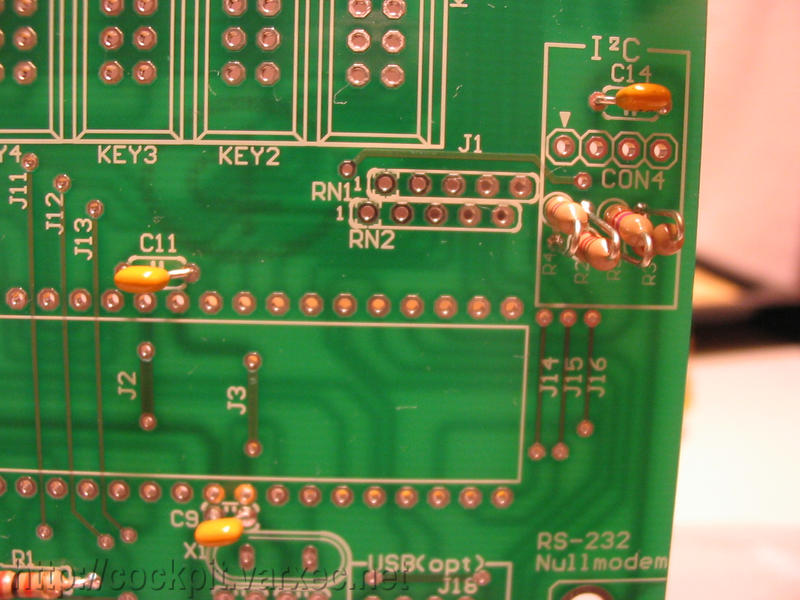 |
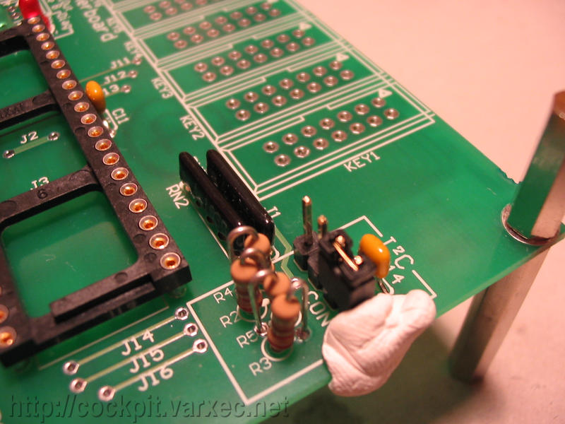
Before we do the IC1 socket, it might be good to add the two resistor arrays (RN1/RN2) first. The resistor arrays have a "common" lead. Its marked with an small "1" on the board (its the leftmost pin in the picture). |
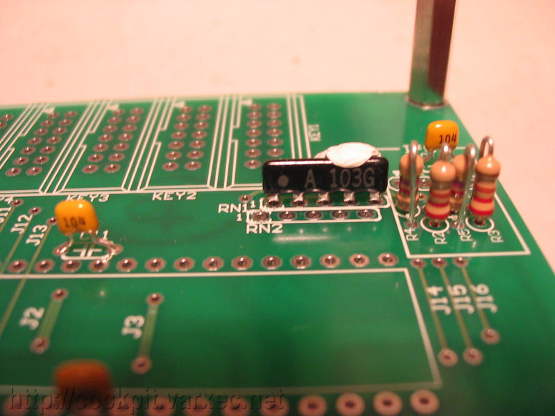 |
On the resistor arrays, the common is marked with a white dot. |
 |
Again, I'm using the removable adhesive putty. |
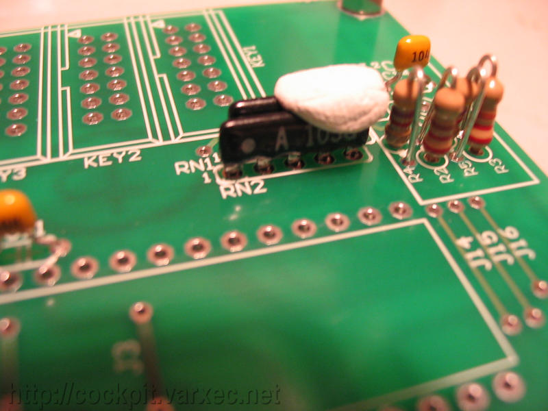 |
The second one, RN2. |
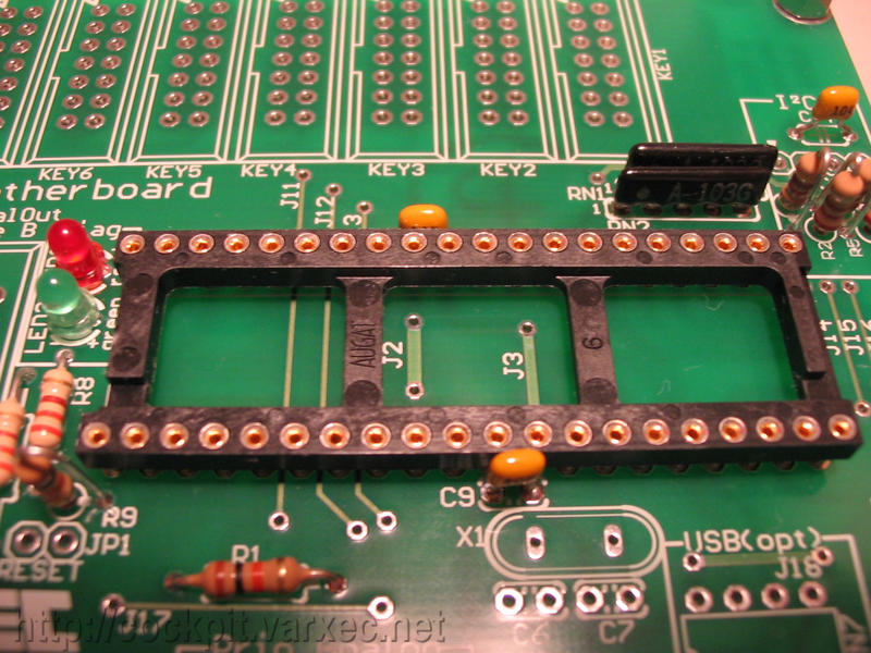 |
And back to the last IC socket, for IC1. Its a bit harder to see with this kind of socket, but pin 1 is on the left. |
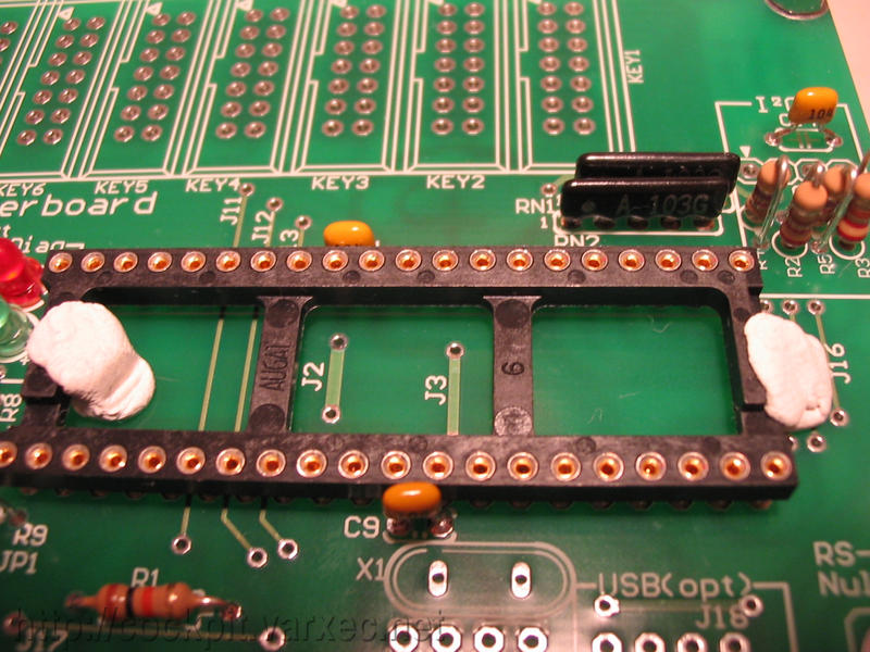 |
Some putty to hold it, then solder. |
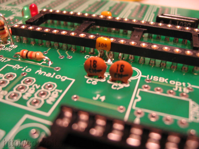 |
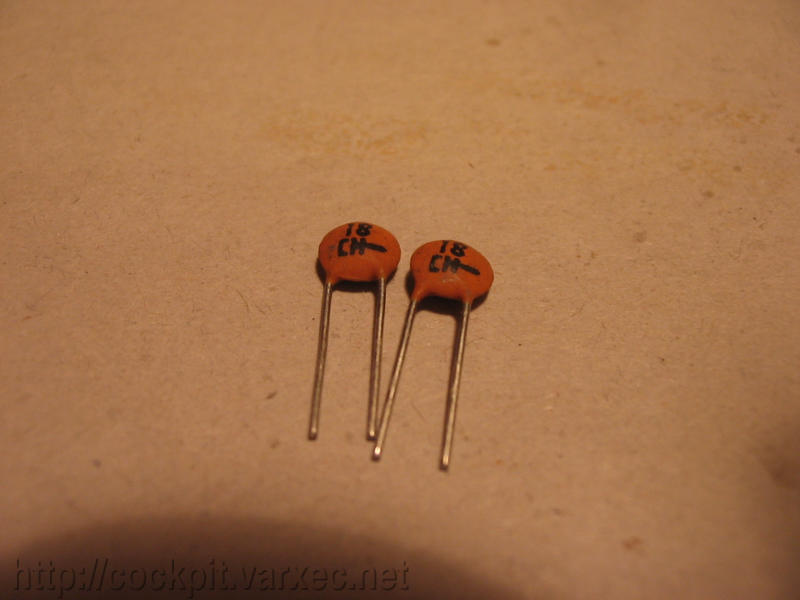
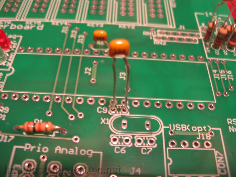
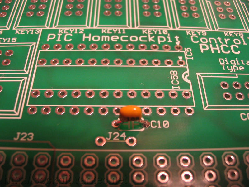
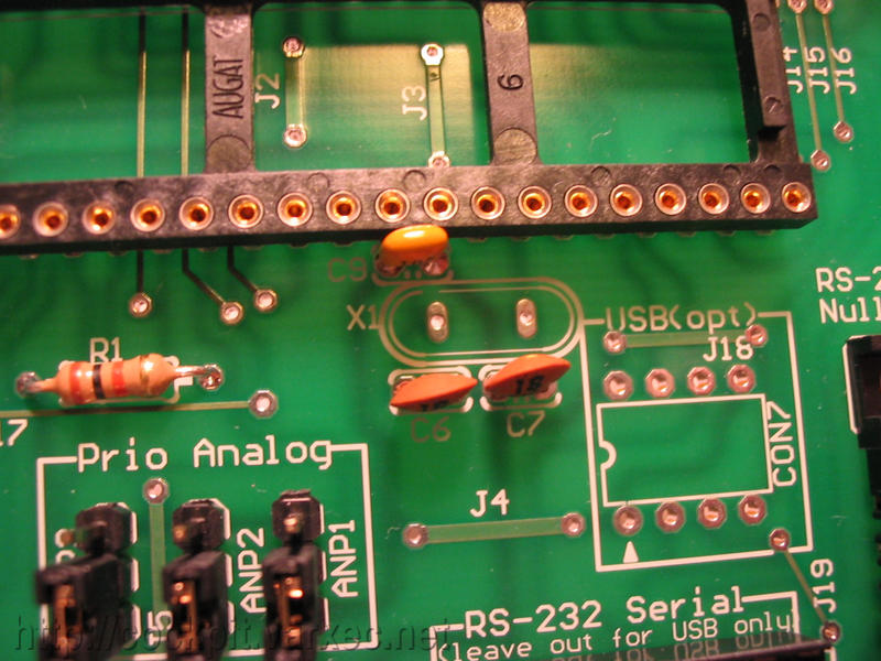
Next are the last two capacitors, C6/C7. They help the crystal oscillator to oscillate. The value is 18pF (pico farads). Higher value caps (up to 33pF) are also ok. These caps are non-polarized. |
 |
The underside. -> Solder. |
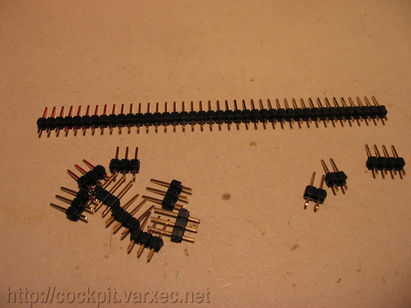 |
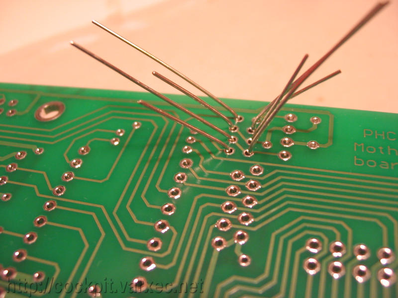
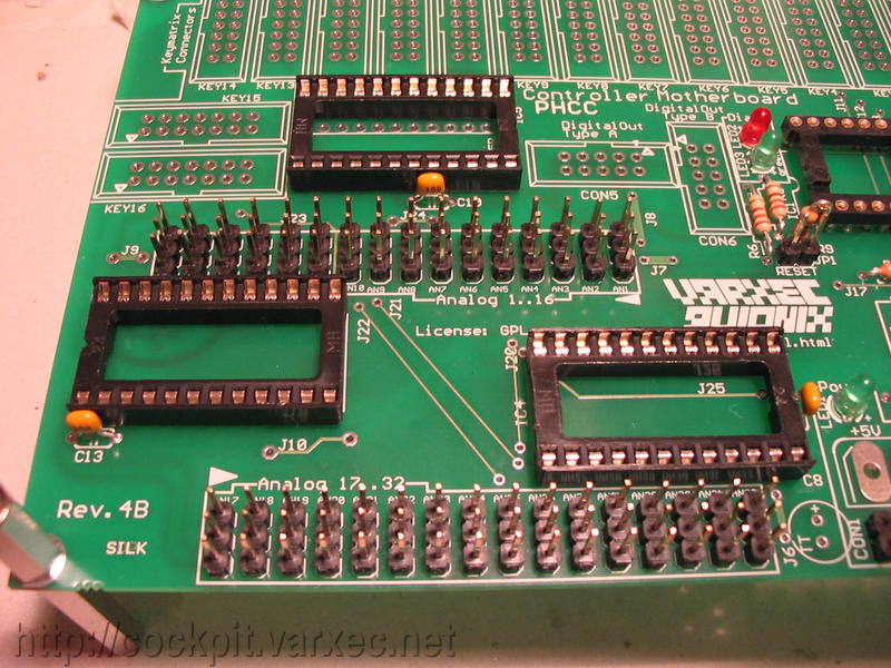
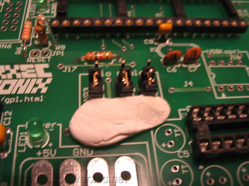
The pinheaders (for CON1, CON4, JP1, ANP1-3, AN1-32) come in longer strips and have to be broken down. |
| We need one 4pin strip, two 2pin strips, and 33 3pin strips. Using plier to break these down might help. | |
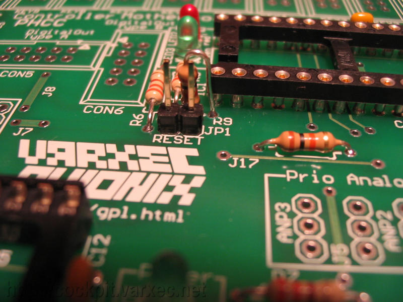 |
The 2pin strips first: JP1 (the reset jumper) and ... |
 |
... CON1, the power supply connector. |
 |
Next CON4, the 4pin ICSP pinheader. |
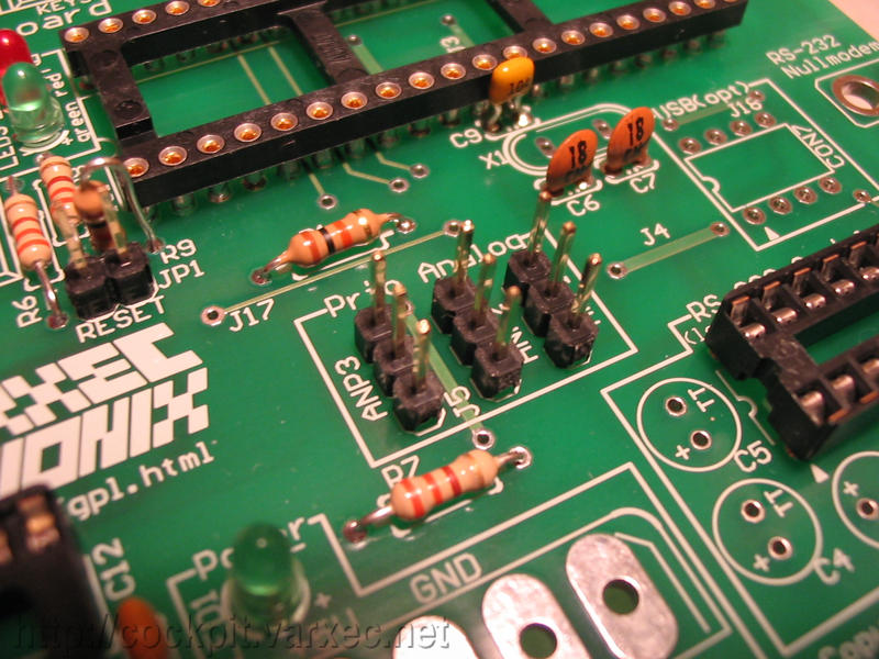 |
Now the three primary analog input channels, ANP1-3, using 3pin pinheaders. |
 |
And the remaining 32 3pinners are for AN1-32. |
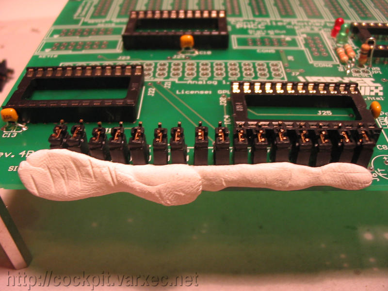 |
Here's how I kept the pinheaders from falling off the board before soldering: I used the jumpers and some putty. (The putty shouldn't get too hot, it starts to smell). |
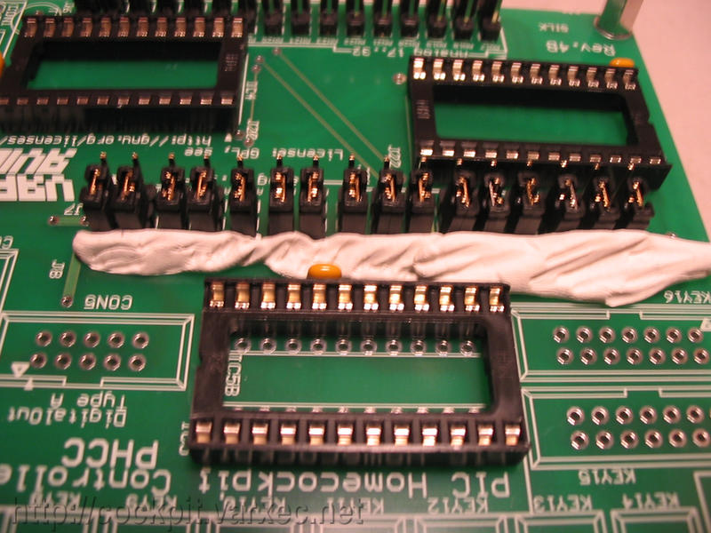 |
The other row. |
 |
CON4. |
 |
ANP1-3. |
 |
JP1/Reset. |
 |
CON1/Power. Dont forget to remove the jumper after soldering. If you apply power via the other connector with the jumper on, bad things will happen :) |
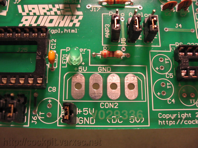 |
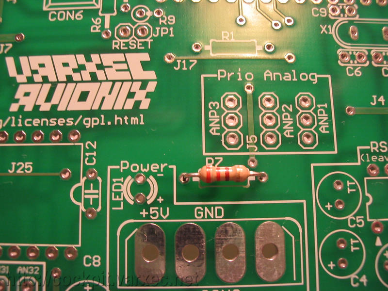
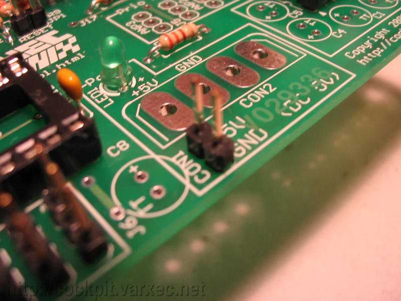
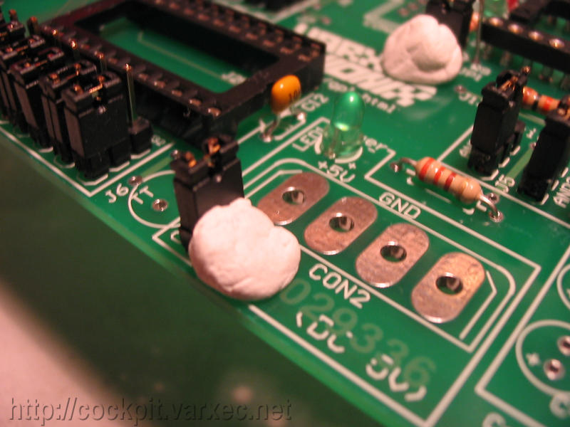
Now the other power connector, CON2. The same type is used on PC harddrives,... This allows it to use PC power supplys for PHCC. |
 |
Putty in action again. |
 |
Moving on to the shrouded IDC type pinheaders. Starting with CON6, the 2x5pins DOB connector... |
 |
... then CON5, the 2x5pin DOA connector. |
 |
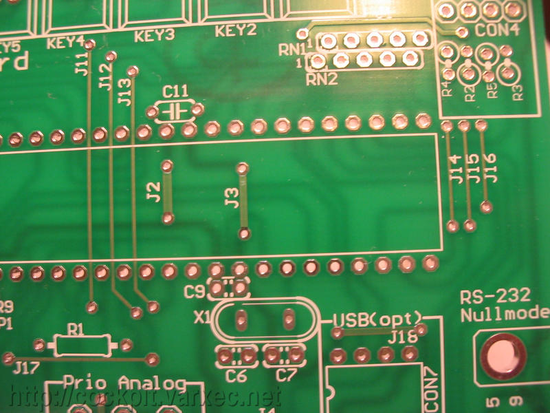
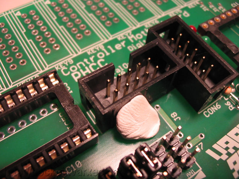
And then the 16 (2x7 pin) keymatrix daughterboard connectors KEY1-KEY16. |
 |
I did these in rows of four, but first soldered only two pins on each connector. |
 |
After all are in place with two pins soldered, ... |
 |
... I soldered the remaining pins. |
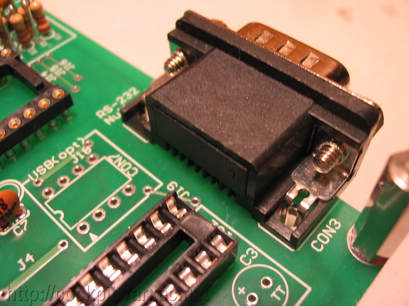 |
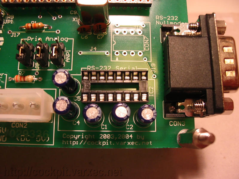
The serial port section is where we focus next. |
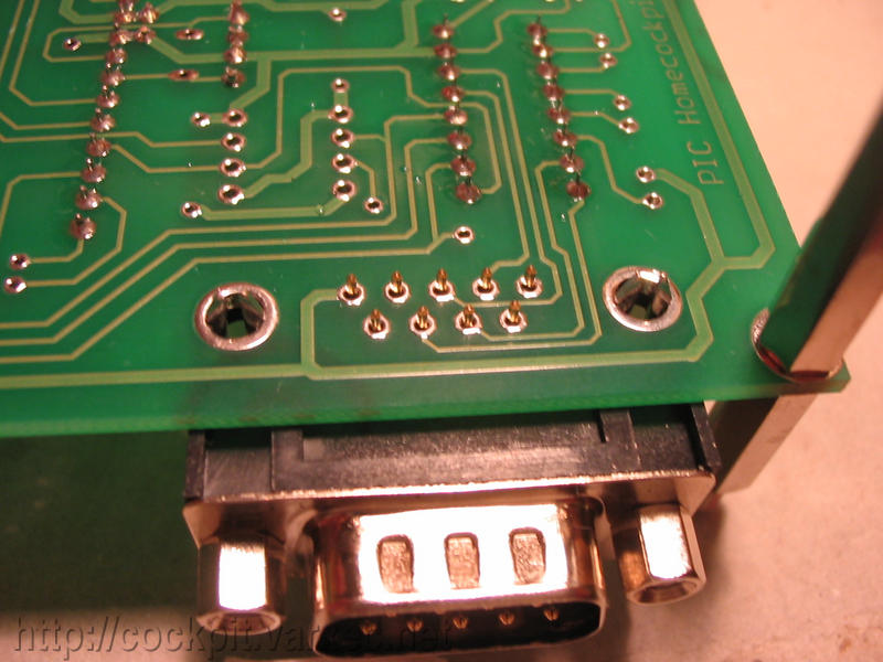 |
CON3, the SUB-D 9pin male connector kept itself in place, so no putty needed here. |
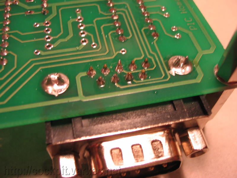 |
... after soldering. |
 |
The end is drawing nearer... now we need to take care of the six electrolytic capacitors. First the four 1uF caps... |
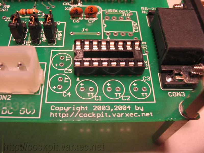 |
... C1-C4. As alreay mentioned, electrolytic caps are polarized and usually the negative "-" is marked on the package. The board on the other hand has "+" marked on it. |
 |
When these are soldered ... |
 |
... continue with C5, the 10uF cap. Same story here. |
 |
It should now look like this. |
 |
The last electrolytic cap, C6, goes here. Again, make sure you get "+" and "-" correct. |
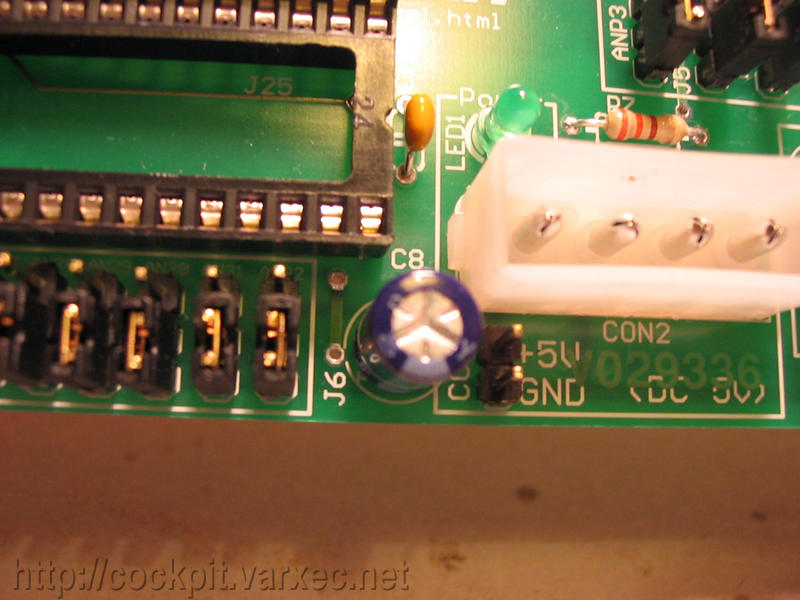 |
The negative side points downwards. |
 |
And finally... the last part, X1, the crystal oscillator. |
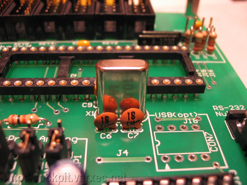 |
Polarity does not matter, but I always put them in so the printed frequency value can be read easily. |
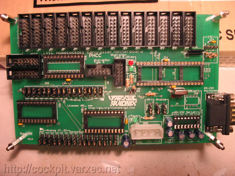 |
Thats it. The board is finished. Now its only waiting for the ICs, the firmware and power. :-) |
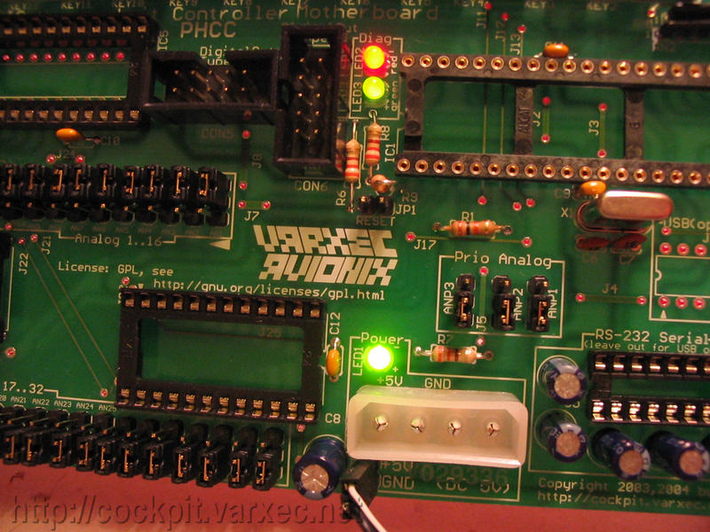 |
But before we put any ICs in, run a dry test. Just apply power to the board. (Doesn't matter which power connector you use). |
| When +5V DC is applied, all three LEDs should light up. The diag LEDs will be dimmer than the power LED, this is OK. | |
 |
If your board passed this first test, put the ICs into their sockets. First IC2, the MAX232. |
 |
Note the notch on the IC. This notes side where pin1 is. |
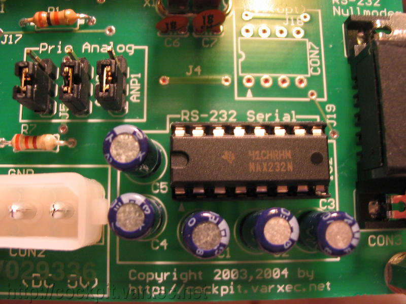 |
The notch points to the left. |
 |
Next, IC5, the 74HCT154. |
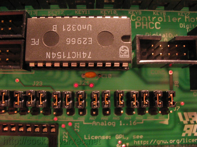 |
Here, the notch points to the right side. |
 |
And IC3/IC4, CMOS/CD4067. |
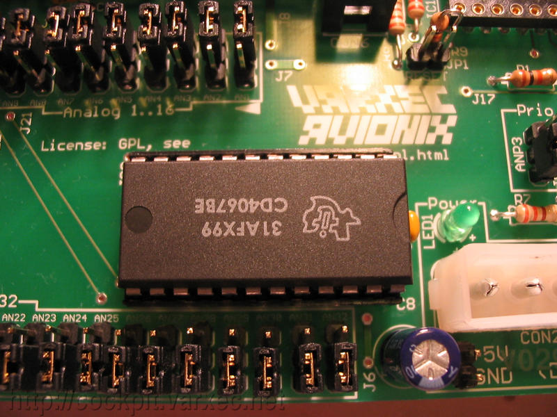 |
IC4's notch points right... |
 |
... and IC3's notch points left. |
 |
It should look like this. |
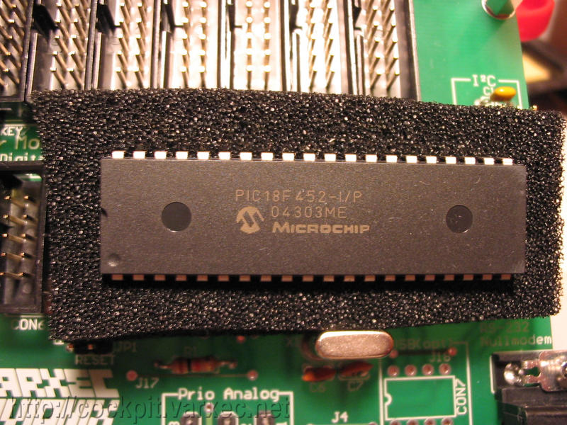 |
Last but not least, IC1, the PIC microcontroller.... but ... before this one is of any use, it needs at least the bootloader programmed in. (The PICs part of the kit are preprogrammed, so the owners of kits can skip this step). |
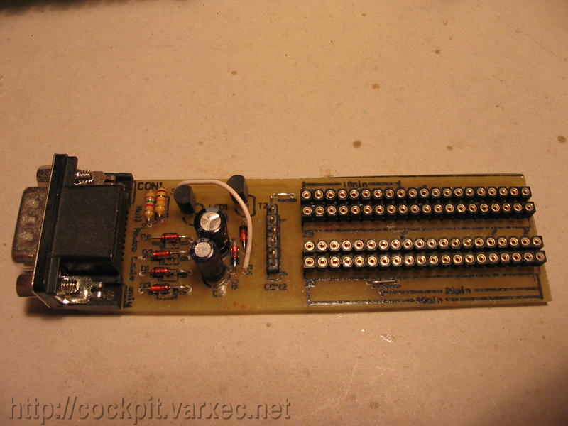 |
My simple JDM-type serial port programmer. |
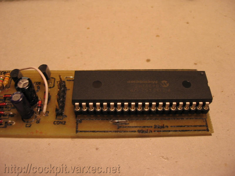 |
The PIC 18F452 loaded up. |
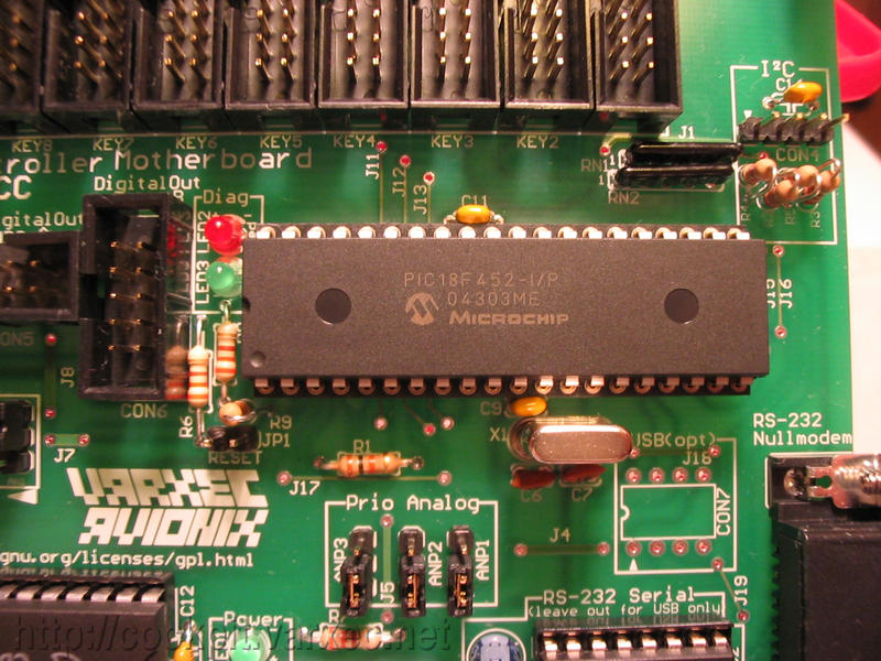 |
The PIC in its final place on the motherboard |
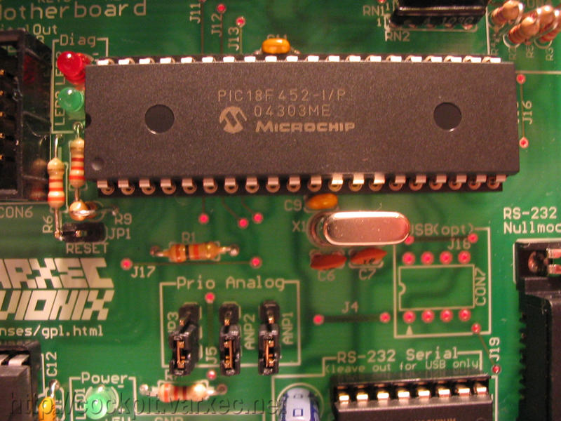 |
A Note about CON7, the USB daughterboard socket (lower right hand corner in this picture): it doesn't make sense to put the IDC DIP8 connector in until you have a USB daughterboard. Actually, it makes sense to add a DIP8 IC socket where the IDC DIP8 flat cable connector can plug into. |
Thats it :)