Assembling the PHCC Daughterboard "DOB_74595+T"
Intro
The Hi-Current Output Daughterboard "DOB_74595+T" can be used eg for
- Lamps, eg cockpit lamps, korry indicators
- LEDs
- DC-Motors
- Relays
- Solenoids
- Fans
-
and a lot more.
Each output is rated 1 Ampere max. continous current. This should be sufficient for most needs. For more, use a relay instead and drive the relay with this board.
Variants
not really a variant, but you have to choose if you want the board to amplify the data signals for the daisy-chained boards. Such an amplification is only needed every few boards, say every 3-4 boards. If you choose to go with amplification then IC3 is needed, otherwise it can be left out and jumper wires added like the component print indicates. For details check further down.
How to connect stuff...
There are two rows of eight screw clamp terminals and each of the two rows has its own power supply screw clamp terminal. The outputs are open collector type. The transistors are low-side switches, meaning that if you eg. want to connect a lamp to it, you would hang the positive side of the lamp to the positive side of the power supply, and the negative side of the lamp to the output screw clamp. Then connect the power supply to the 2pin screw clamp: negative side to "GND REF", positive side to "REF OC". The only purpose for the "REF OC" is to provide a path the fly-back voltages of inductive devices (eg. relays, solenoids, motors). Even if you plan to drive only non-inductive devices, it is highly recommended to connect "REF OC".
This board can drive voltages up to 80V. The transistors used determine the actual max. voltage. The BC635 drives up to 45V, the BC637 drives up to 60V and the BC639 drives up to 80V.
Assembly
First start with the smaller components and work your way up to the bigger ones like sockets and connectors. This helps at places where the bigger stuff might get in the way of soldering smaller parts.
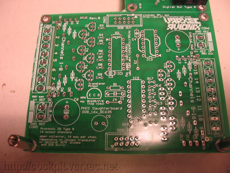 |
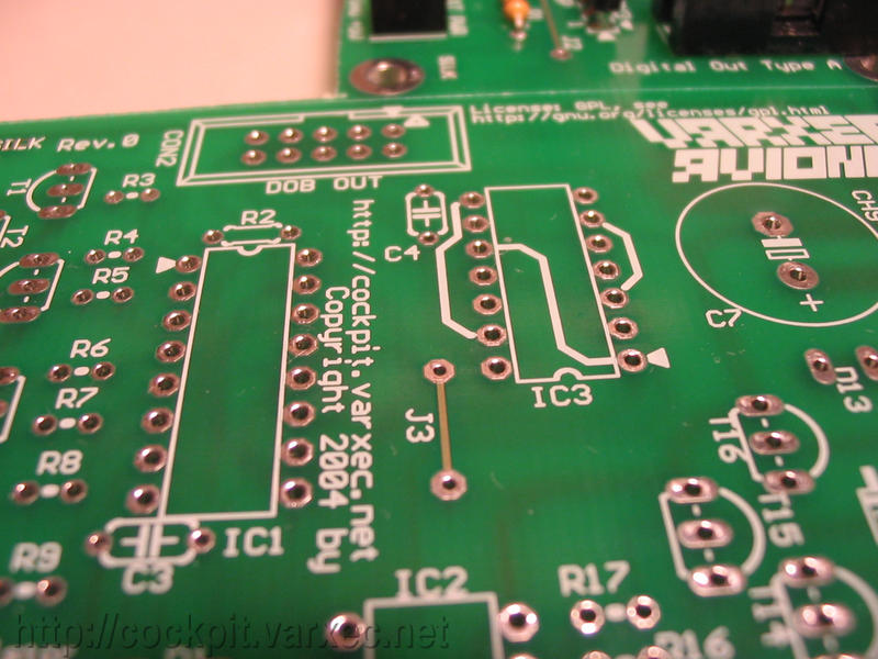
The bare board. |
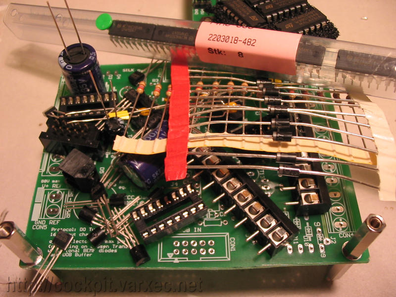 |
All the needed parts. |
 |
Start with the Jumper wires J1-J4 if you have a single sided board. The board in our pictures are double-sided, so this step could be skipped. Note that J1 and J2 need some thicker wire since they can carry a few amps of current. |
 |
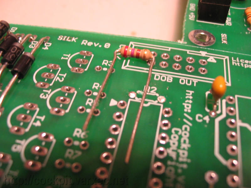
Start with the horizontal resistors, R1, R2, R10. Using a device to bend wires to standard widths is practical but not required. It can make your life easier. |
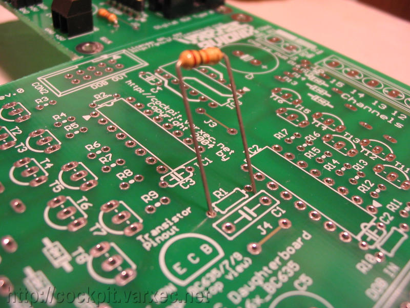 |
Put in those three resistors. (Note that I messed up R2, so please don't wonder about R2 and C3 exchanged in some of the following picures.) |
 |
R2 and R10 put in place. |
 |
Note that I messed up R2, so please don't wonder about R2 and C3 exchanged in some of the following picures. See next picture (taken while fixing the mess-up) for R2 |
 |
R2 right next to IC1. Disregard C4 seen to right. This picture was taken when fixing the R2/C3 mess-up |
|
|
The spacing of R2 has been changed in Rev.0B. So your R2 will look nicer. |
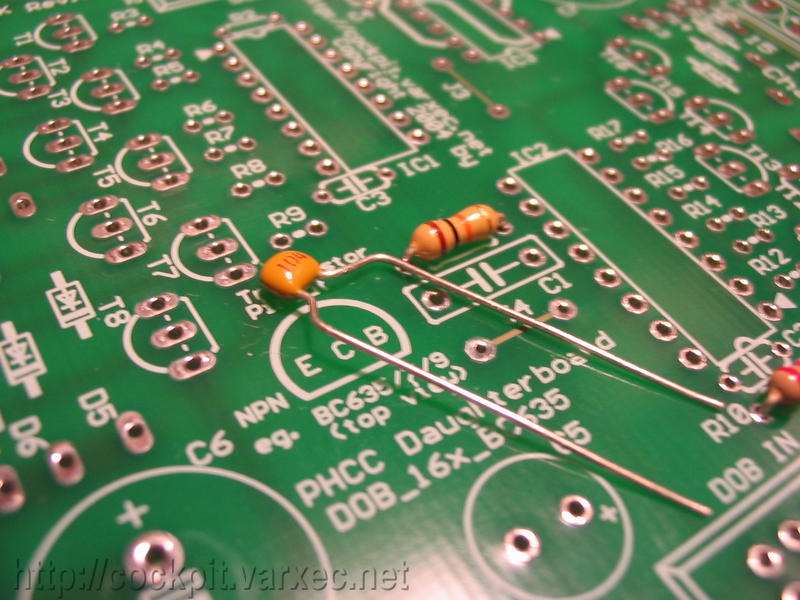 |
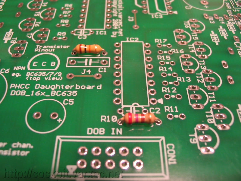
Before soldering the three resistors, I also put in the ceramic capacitors, C1-C4. All are 100nF. This value is not critical, so similar values can be substituted. |
 |
Note that C1 has a wider pin spacing than the others, so it has to bend its legs outward a little. |
 |
C1-C4 added this shows where I started to mess up, C3 sits in R2s place. don't do this |
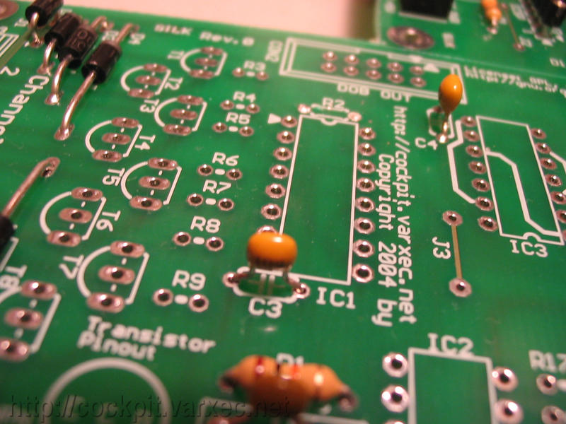 |
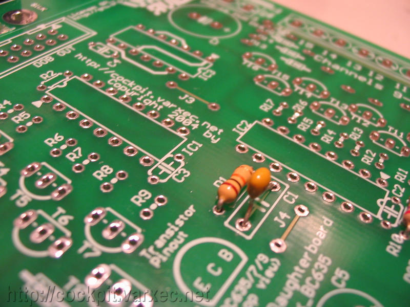
This is where C3 should go. |
 |
C3 and R2 in their correct places. Some of the follwing pics show them still wrong, don't worry |
 |
To keep the parts from falling out when the board is turned around for soldering, bend their leads outwards. |
 |
Now solder. |
 |
And remove the excess lead length. |
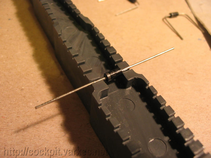 |
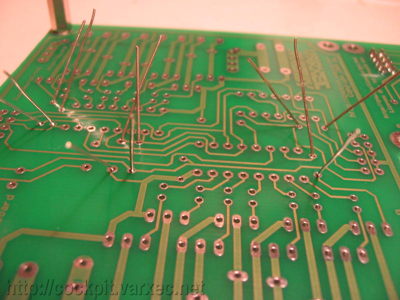
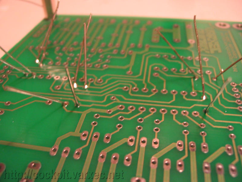
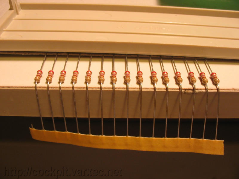
Next are Diodes D1-D16. Types: 1N400x, eg 1N4007 Again, using this tool helps. |
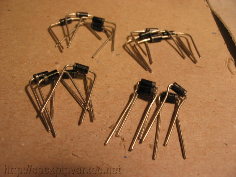 |
All diodes bent to fit. Four different lead pitches, four diodes each. |
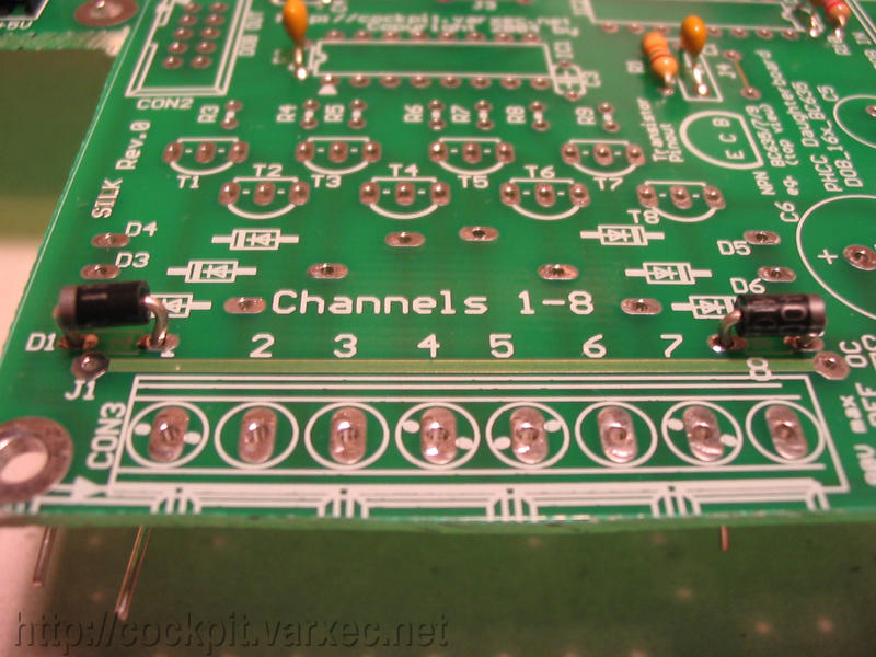 |
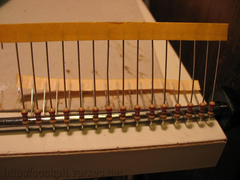
First put in D1, D8, ... |
 |
and D9 and D16 on the upper row. |
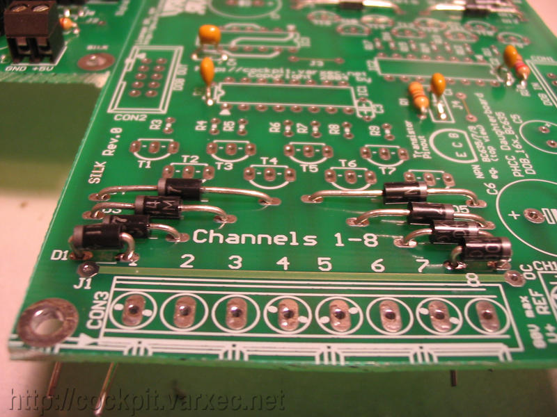 |
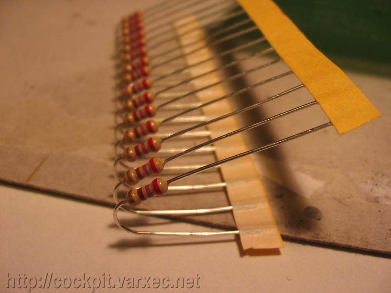
Work your way up the diode pitch sizes ... |
 |
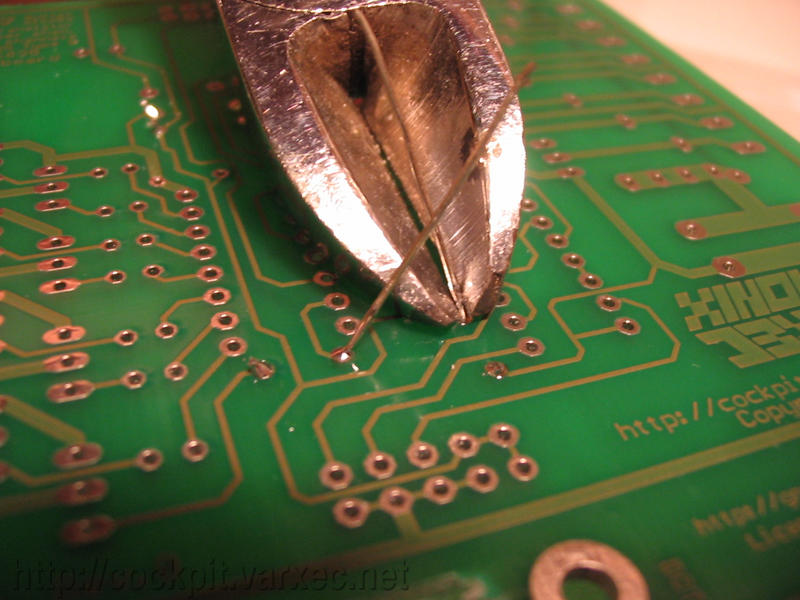
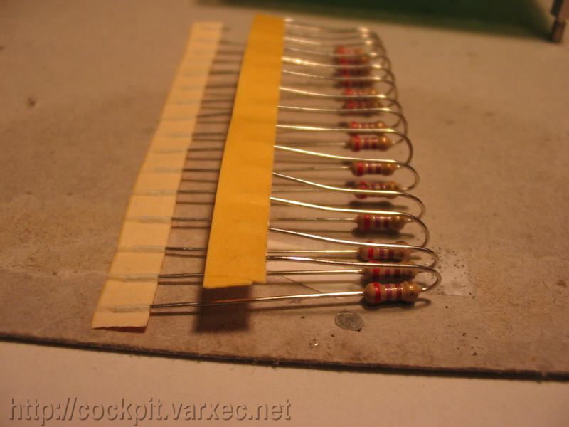
... until you have all 16 diodes in place. Then solder and remove excess lead lenght. |
 |
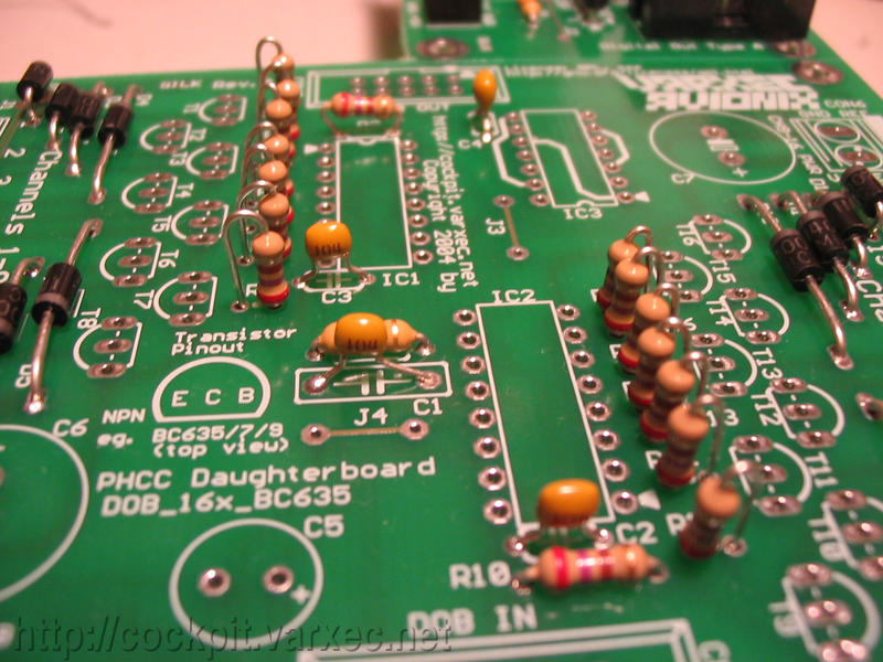
Now bend the vertical (standing) resistors, R3-19 and R11-R17. I was lazy and tried all 15 of them at once. |
 |
first step: 90 degrees ... |
 |
second step, to 180 degrees using a round object ie. a rod. |
 |
Not quite 180, but the rest can be done by hand. |
 |
There we go. |
 |
Put them in as shown. |
 |
This keeps'em from falling out before soldering. Now solder and cut. |
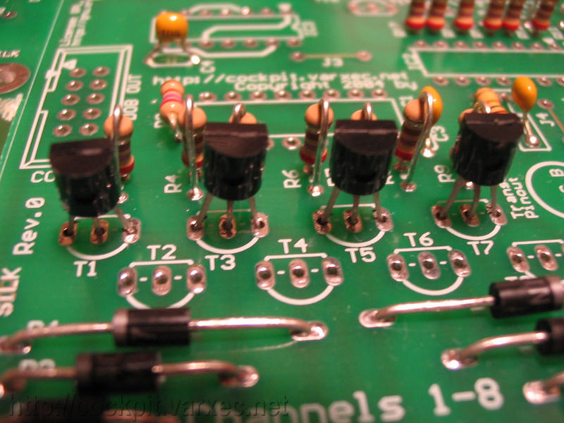 |
Next are the transistors T1-T16. You might have to bend their leads outward a bit to make them fit the holes. Start with the row that sits next to the resistors, ie. the odd numbered transistors: T1,T3, ... T15 |
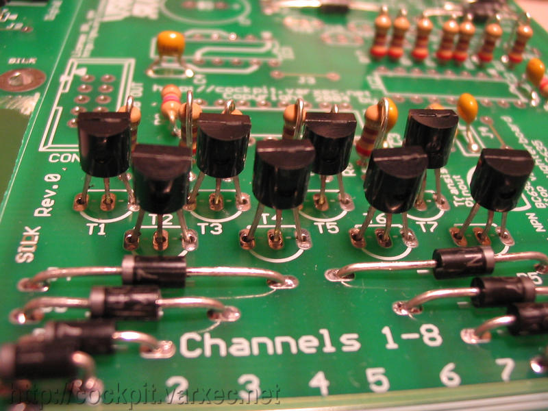 |
Then the even numbered transistors. Solder and cut. |
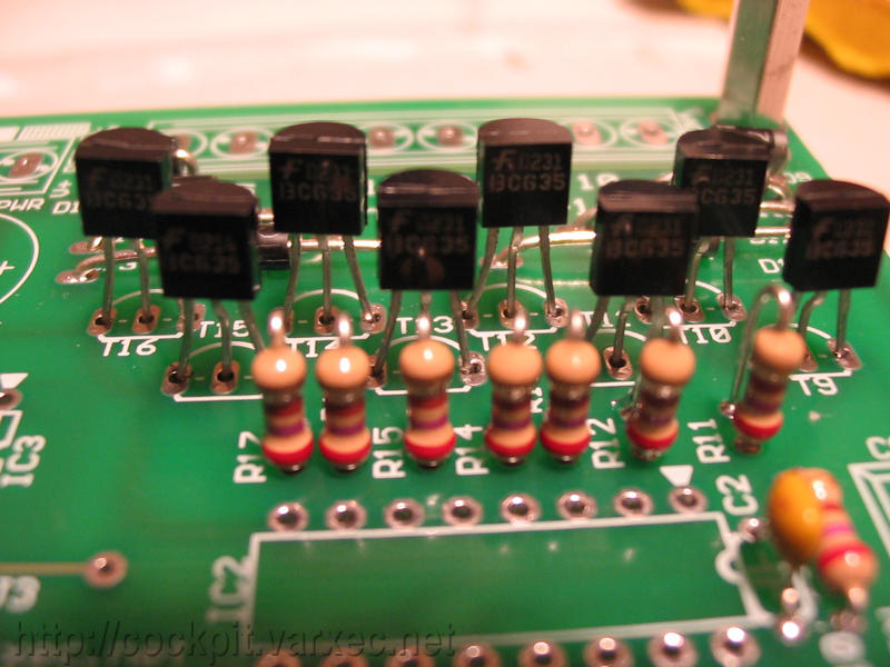 |
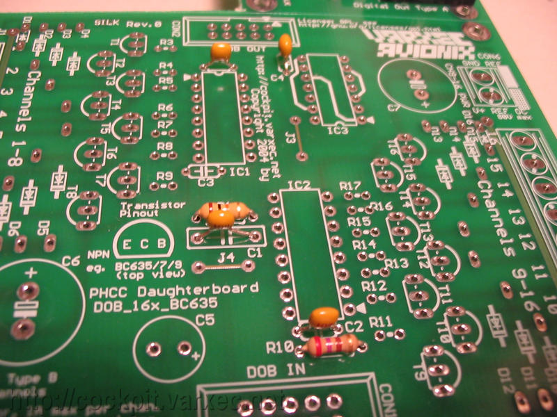
Front view of T9-T16. Make sure the transistors are like in the picture. The component print on the board helps to get the orientation right. Don't push them too far down, this might damage the leads. It also helps heat dissipation if they sit a bit away from the board. |
 |
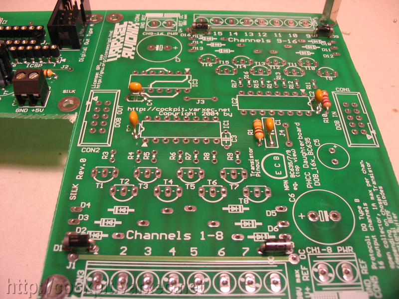
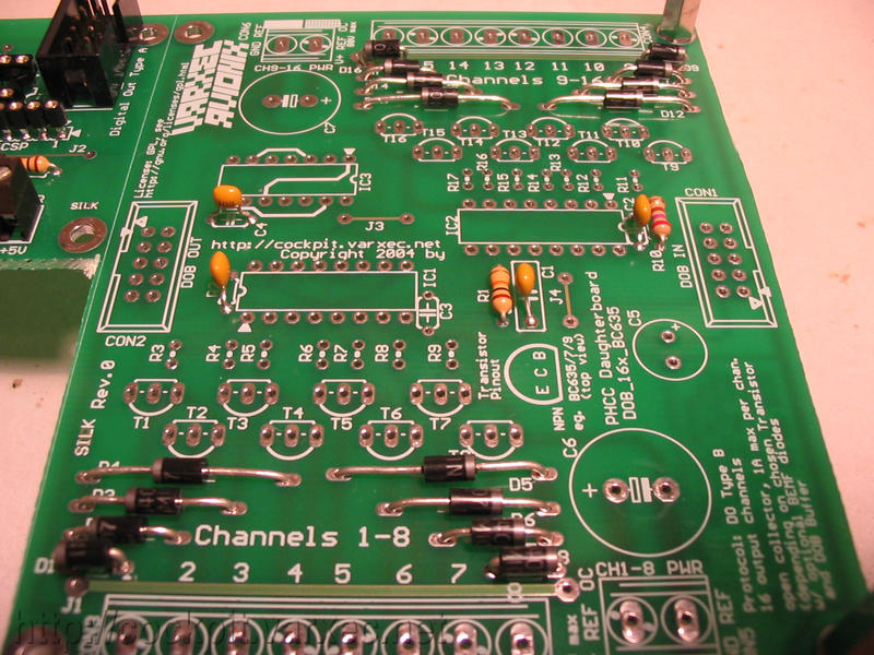
This shows our current progress. |
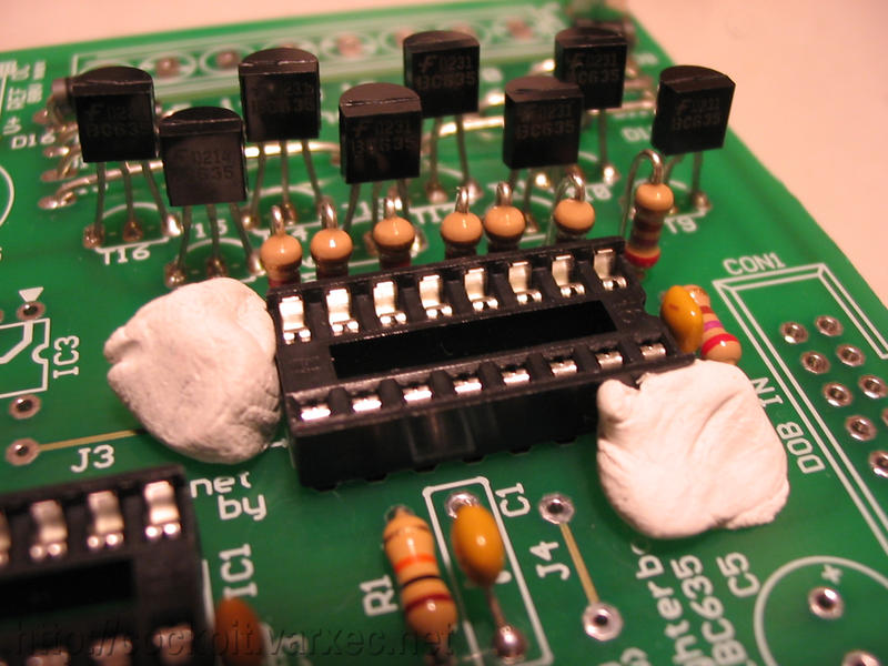 |
The IC sockets can be easily held in place with the help of plasti-tak(R) (removable adhesive putty). Put in the sockets for IC1 and IC2. |
 |
If you want to build the variant with signal amplifier, then also add the socket for IC3. |
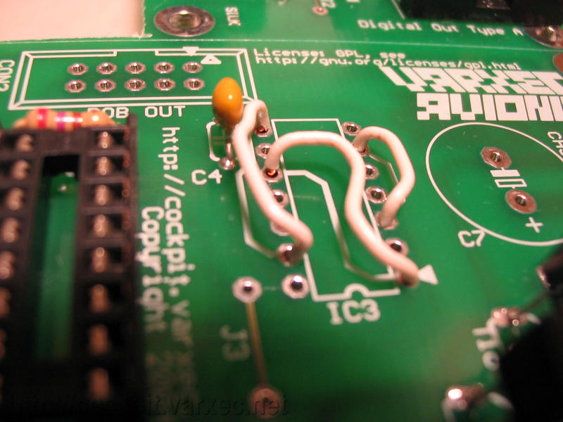 |
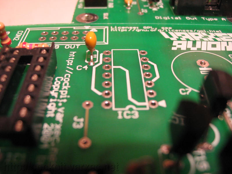
Otherwise jumper as indicated. |
 |
Another view. |
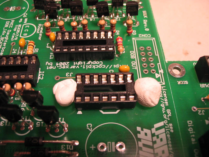 |
In this example I built the variant with signal amplifier, so I used a socket for IC3. Now solder all the IC sockets. |
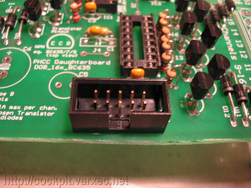 |
Move on to the two DOB connectors, CON1, CON2. Make sure you put them in the right orientation. The cut-out always points away from the board. |
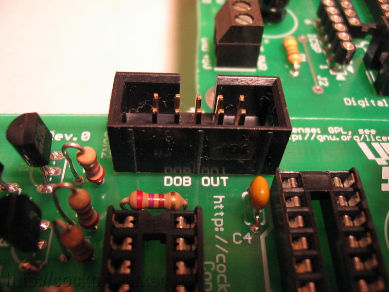 |
CON2. Solder both. |
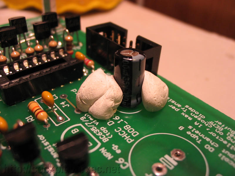 |
Now its the turn for the smaller electrolytic cap, C5. Again, the plasti-tak method helps here. |
| Solder. | |
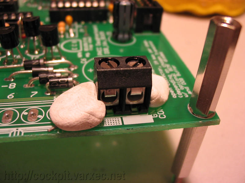 |
Now the screw clamps, starting with the two-pin kind for the power supply: CON5,CON6 |
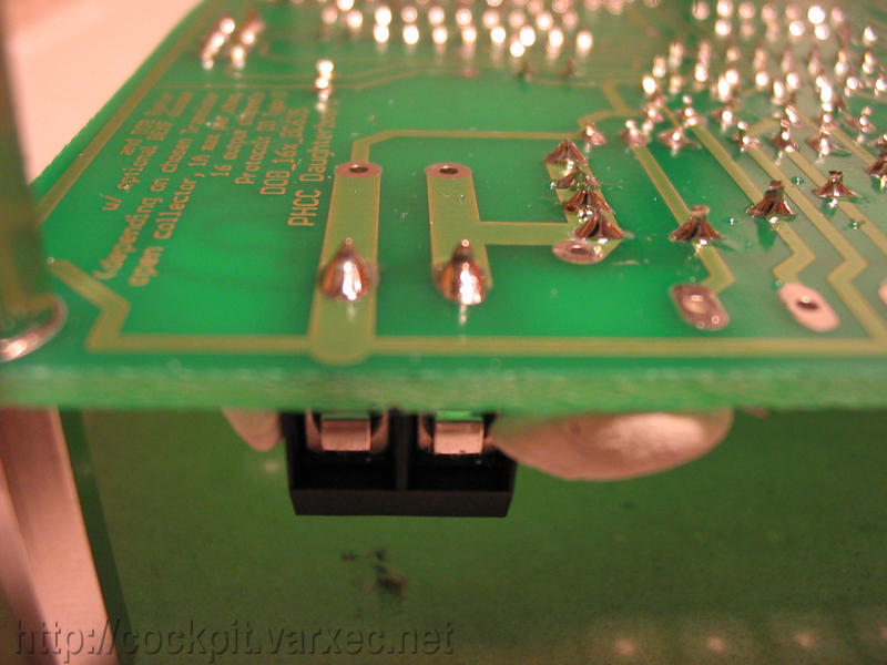 |
Solder. |
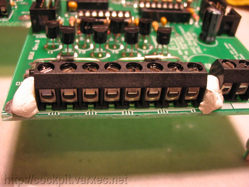 |
Then move on to then 8-pin screw clamps for the outputs: CON3, CON4 (these are sinking 'outputs', so always connect the negative side of your device to these clamps, positive goes to the positive supply thats also connected to "REF OC" on CON4/5) Solder. |
 |
The last two parts are the big electrolytic caps, C6, C7. Solder. |
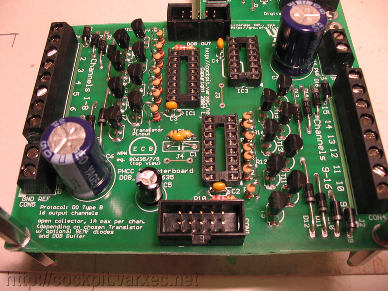 |
All parts soldered. All thats missing now is ... |
 |
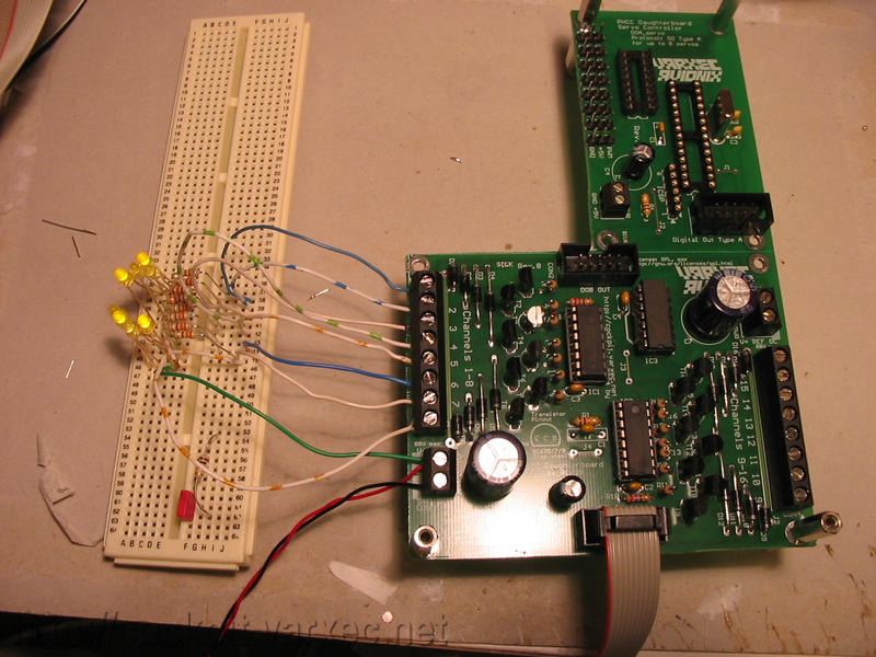
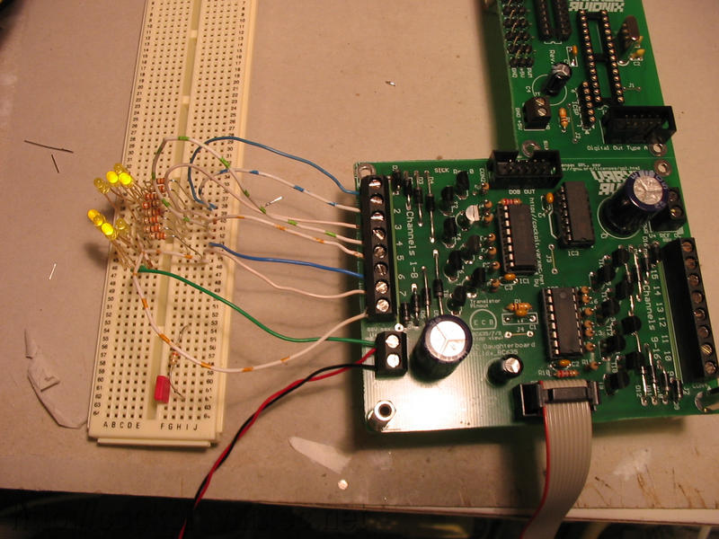
... the ICs and the connection to the PHCC motherboard. |
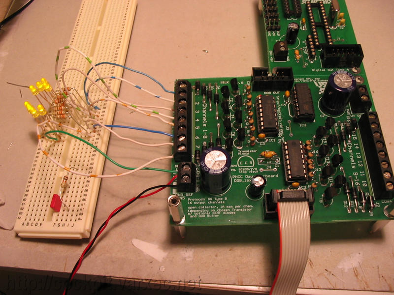 |
A first test with LEDs. All on. |
 |
every other on. (hexadecimal: 0xAA) |
 |
every other on, second way of doing it. (hexadecimal: 0x55) |
Thats it :)