Assembling the PHCC Daughterboard "DOA_AnOut1"
Intro
The Analog Out Daughterboard "AnOut1" can be used eg for:
- Meter movement (d'Arsonval) instruments.
- dimming of incandescent lights and LEDs
- speed control for small (<500mA) DC motors (needs external flyback diode)
- eg. for fans
Variants The 16 output channels can be split (in any ratio) between:
- simple trim pot output stage, and
- transistor output stage
The first type is primarily for d'Arsonval movements and can source up to 25mA, while the second type is designed for light dimming and speed control applications. The transistor chosen for the second type.
In the following picures, the ratio used is 3:1, or in other words: 12 trim pot outputs and 4 transistor outputs. Among the 4 transistor outputs, two use the BC547 and two use the BC337.
Ouputs numbering 1-12 are the ones using precision trim potentiometers at 100kOhms and outputs 13-14 use a BC547 based transistor stage while outputs 15-16 use BC337's.
You can choose whatevert suits you, including 'all transistor' or 'all trim pot' output stages. No changes to the software are necessary.
How to connect stuff...
DOA bus to CON1.
... to trim pot outputs
positive side of your eg. d'Arsonval meter connects to the output pin, the negative side has to connect to ground. \ Since no connectors (apart from Ext. Pwr) for this are on the board, you have to do this yourself.
... to transistor outputs
The positive side of your eg. lamp/motor should be connected to your pos. supply rail \ (which can be different from the +5V board supply, as long as the board's GND and your external supply's GND are connected). \ The negative side should connect to the transistor output. This output type is commonly called "open collector". \ The maximum voltage as well as the max output current depends on the transistor chosen. For example:
- 45V/100mA for BC547 based outputs
- 45V/500mA for BC337 based outputs
For further details see docs.
Assembly
First start with the smaller components and work your way up to the bigger ones like sockets and connectors. This helps at places where the bigger stuff might get in the way of soldering smaller parts.
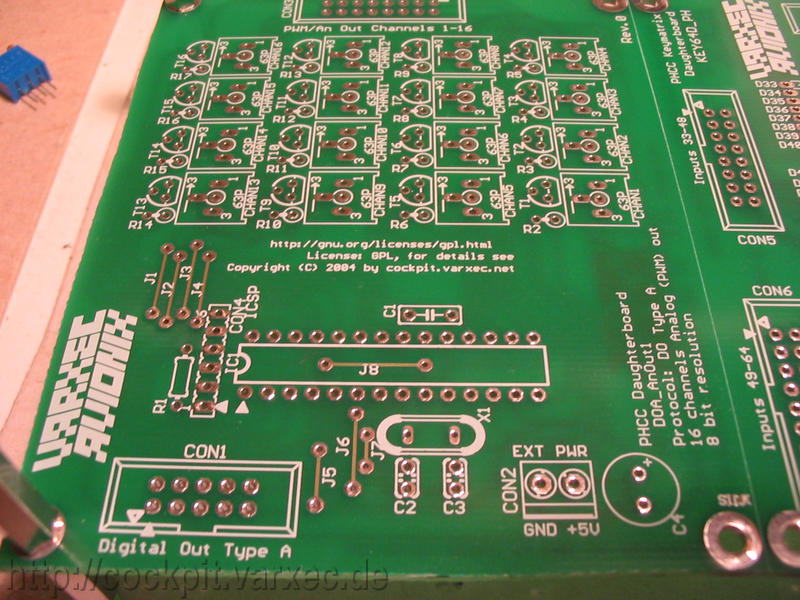 |
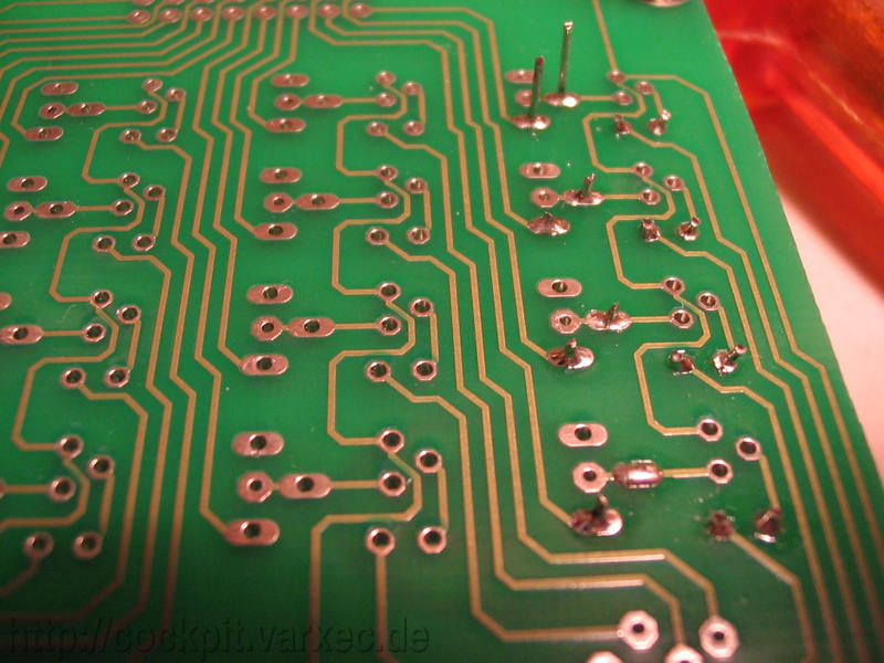
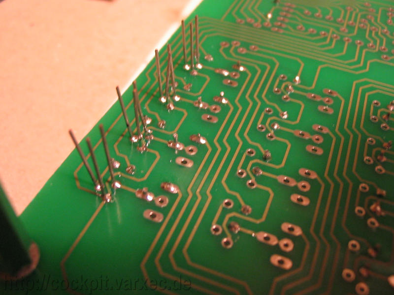
The bare board. Note that in these pictures, the board is actually part of a panel of more than one board. In this case, a Key64D_PH is right next to it. |
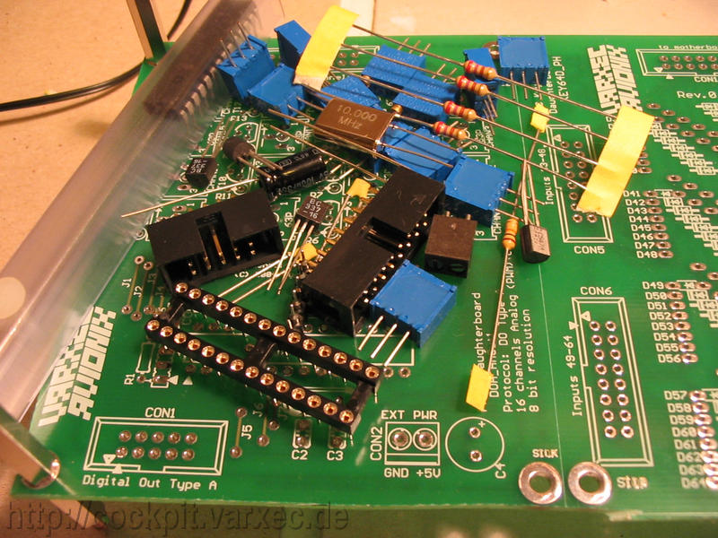 |
All needed parts can be seen here. |
 |
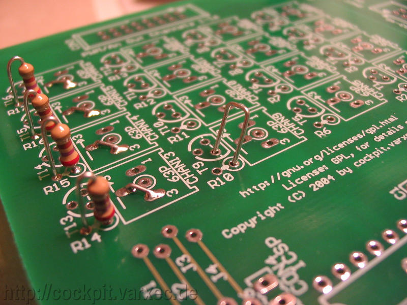
We'll start off with the resistors. For each transistor output stage, we need one resistor with a value of 270 Ohms. Thus, four resistors are needed for the chosen configuration (12 trim pot/4 transistor output stages). These will be soldered in a standing position so bend one lead of each resistor as shown. |
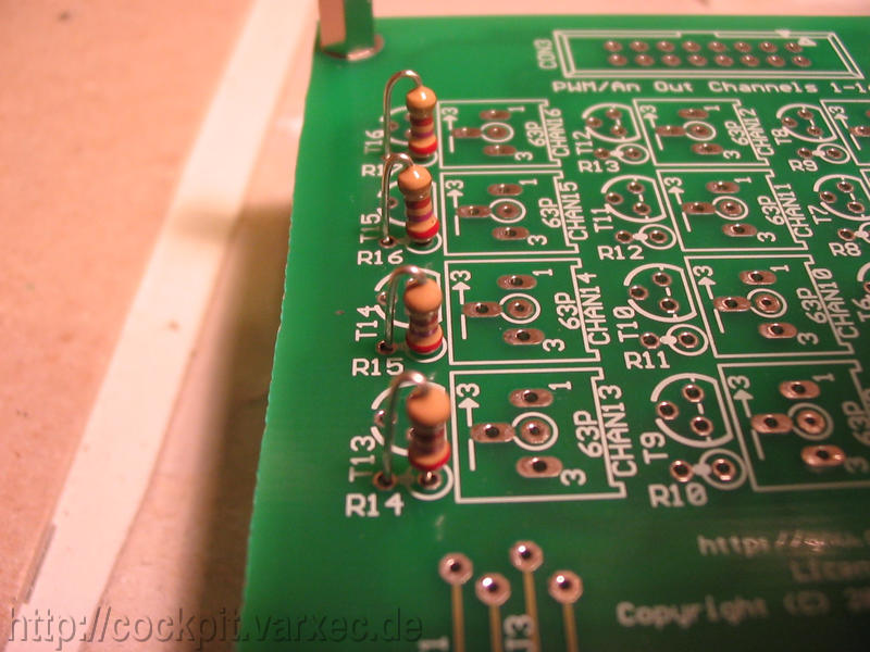 |
Output channels 13-16 will be transistor output stages, so those resistors will be R14-R16. |
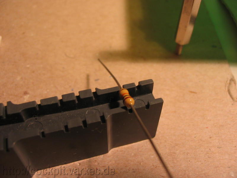 |
The only other resistor we're gonna need for this board is R1, the pullup resistor for the PICs MCLR pin. The value of 10k is not critical, higher values up to 100k are also ok. I use this helper tool to bend the leads. |
 |
Horizontally mount R1 as shown here. |
 |
Bending the leads like this helps the resistors to stay in place turning the board around for soldering. |
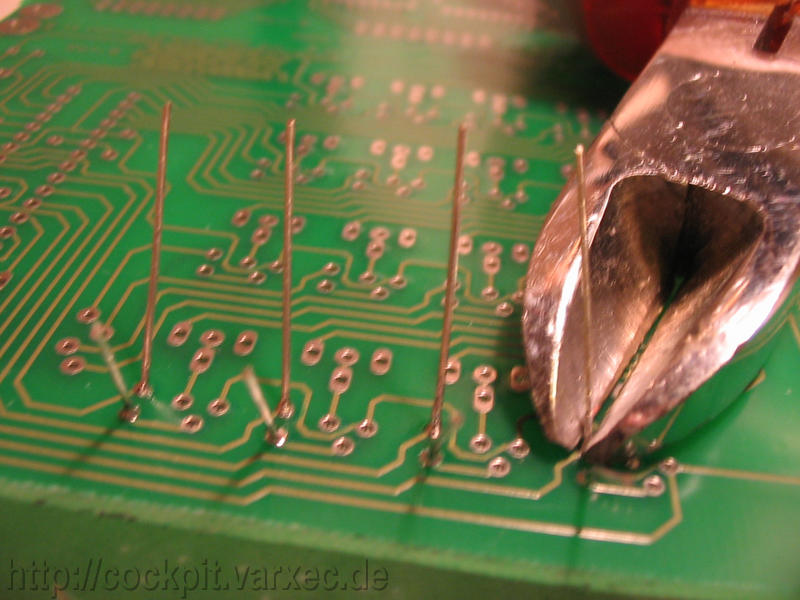 |
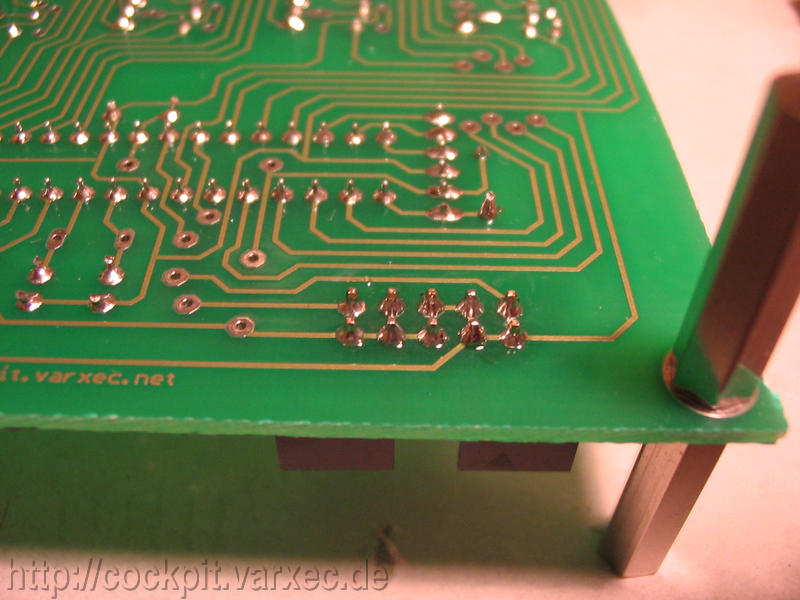
After soldering, use a wire cutter to cut off the leads above the solder joint. Be careful not to pull too hard since it might pull off the whole trace from the board. |
 |
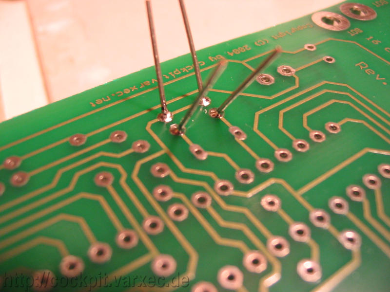
Don't throw away the cutoffs since we'll need them soon :) They make perfect jumper wires, and since those leads are usually tinned, its easier to solder than copper wire. |
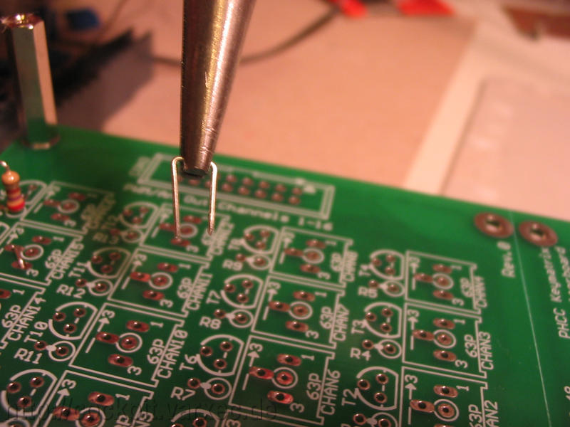 |
Here's how we are gonna use the cutoffs: Bend them like shown so that they'll fit as a jumper, see next picture: |
 |
For those outputs that are gonna be transitor outputs, we need to "bridge" the place where the trim pots would have gone. The bridge will short circuit pin 3 and pin 2 of the trim pot. |
 |
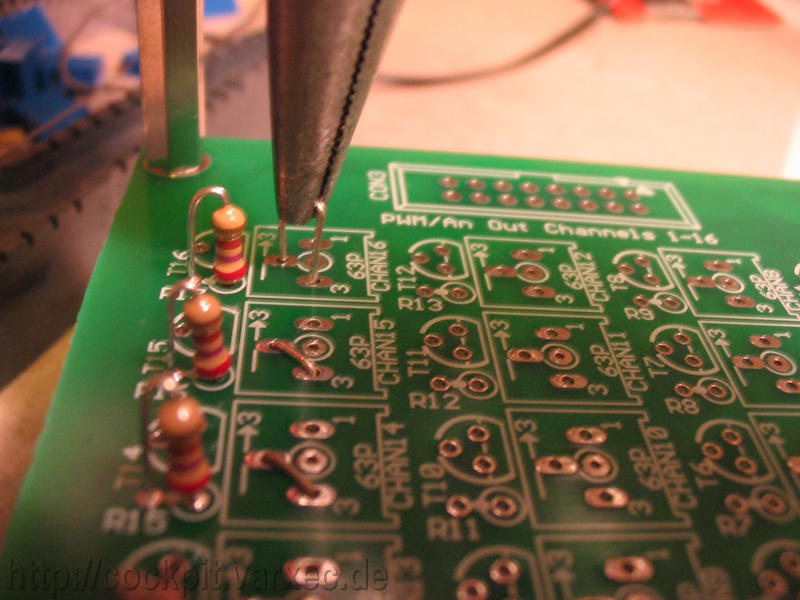
Do this for all outputs you want to use with transistors. |
 |
Solder and cut off excess lead lengths. |
 |
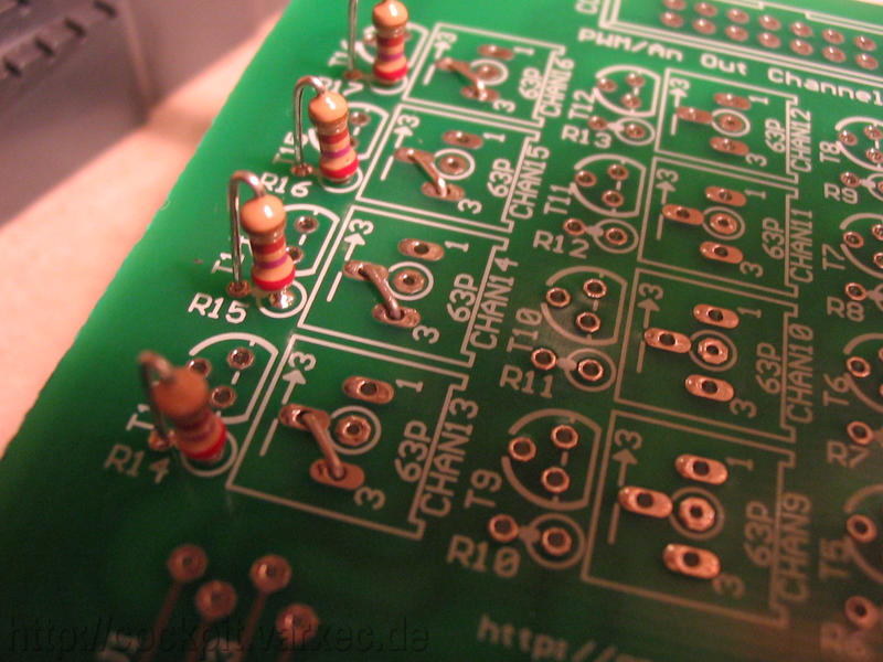
Now move on to the trim pot output stages. Here we need to do something similar, short circuit where the resistor and transistors would go. |
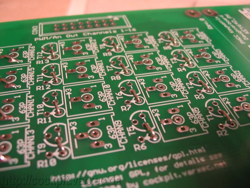 |
Do this for all trim pot outputs. |
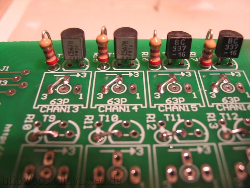 |
Continue with the transistors (T13-T16) themselves. I've used small signal transistors, in particular the BC547 and the BC337. For people where those european transistor types are hard to obtain, refer to the bill-of-materials files for alternatives.Important are the pinouts of the transistors: collector-base-emitter, from left to right in this picture. (The BC547's even have the C,B,E pinout printed on them). |
 |
Solder the transistors. |
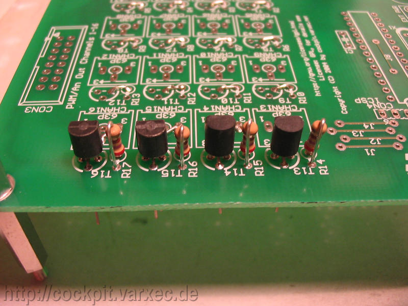 |
Transistors soldered, seen from the back. |
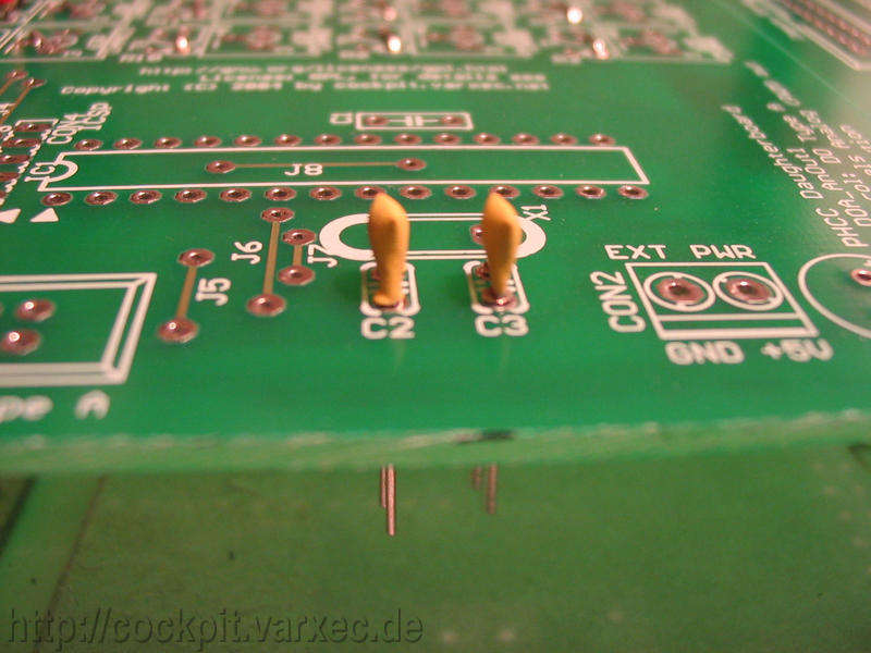 |
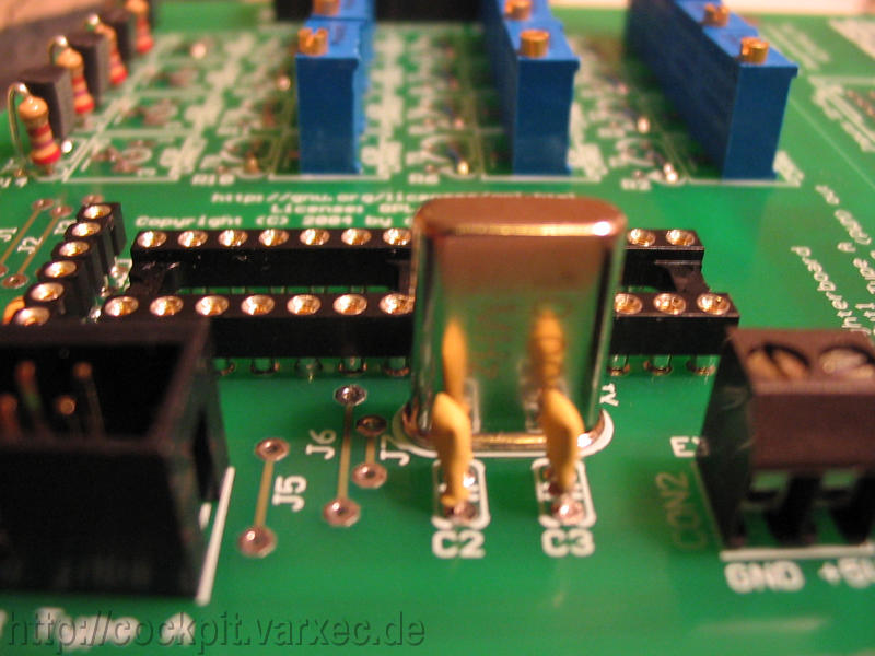
Moving on to the capacitors: C2 and C3 are 18pF ceramic caps. They are needed for the crystal oscillator. Tantalum kind caps should work as well. 18pF are not super critical. Values from 15pF to 33pF should be ok according to the datasheets. |
 |
Bending the pins outward a little before soldering keeps them from falling off the board. |
 |
The blocking capacitor, C1, for the PIC is next. This is a 100nF ceramic cap. I'm using a X7R here. |
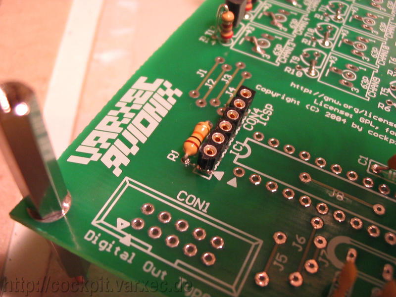 |
Now we move to some bigger parts, first, CON4, the ICSP connector. CON4 is optional but leave it out only if you know you'll never reprogram the PIC in the circuit. |
 |
The best way to keep the part falling out when you turn the board upside down for soldering is to use removable adhesive putty (Plasti-Tak(R)), plasticine or something similar. Just make sure it doesn't get too hot as it might give off some nasty fumes and removing the remains is harder. |
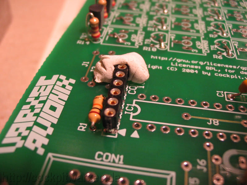 |
Here's how I use the Plasti-Tak(R) to hold the ICSP connector. |
 |
Tacking it at one end is usually enough. |
 |
As you can see, it won't fall off :) |
|
|
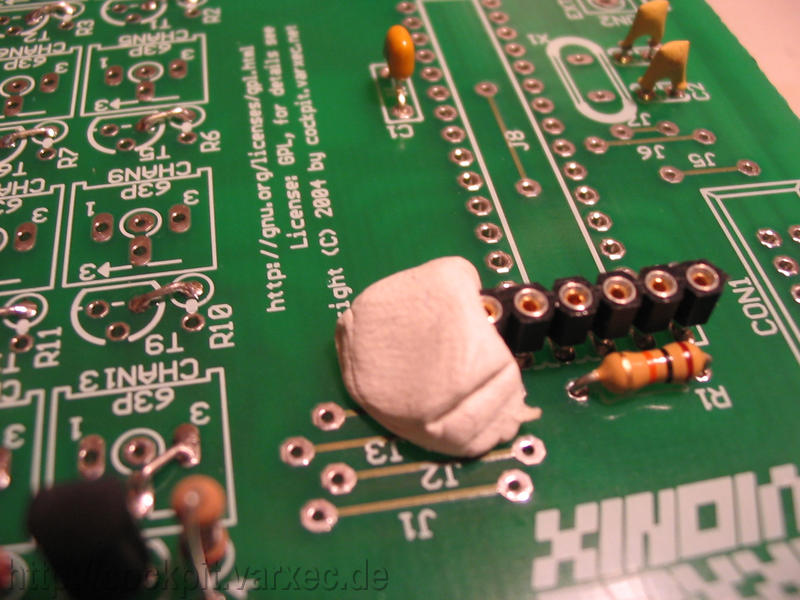
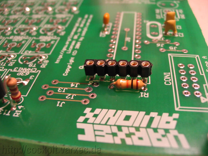
After soldering, you can remove the Plasti-Tak(R) or whatever you used. |
|
|
We use a similar method with the next part, the socket for IC1 (the PIC). Instead of one 28pin socket, you could also use two 14pin sockets as they are more common. |
 |
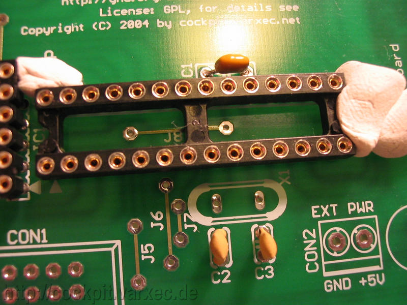
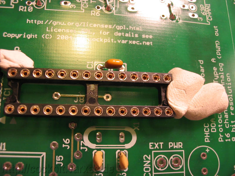
Before you solder the socket, you might have to add a jumer wire, J8, if you don't have a double sided PCB like I do in this picture. And while you are at it, do the same for J1-J7. |
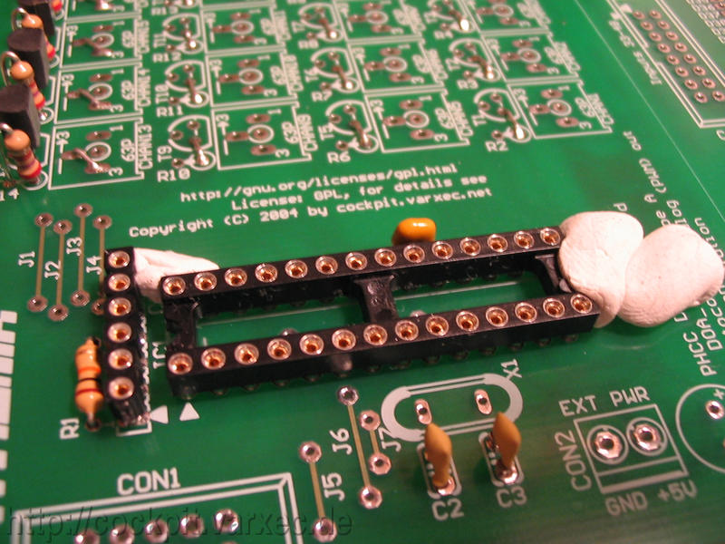 |
Now we can fix the socket in place using two small blobs of Plasti-Tak(R), turn the board around and solder the IC socket. |
 |
Its now time to add the trim pots. In my case, twelve of them, CHAN1-CHAN12. |
 |
I decided to fix and solder them four at a time... |
|
|
... again using Plasti-Tak(R). |
 |
See, they don't fall out :) |
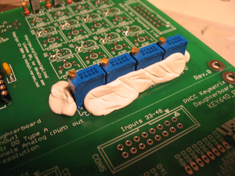 |
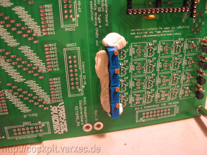
After we soldered all of them in place, it should look something like this. |
 |
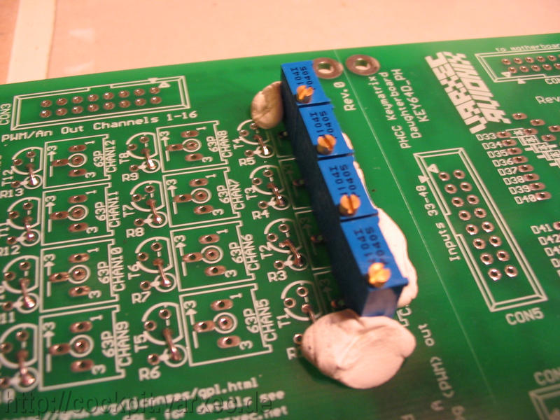
CON2, the Ext. Pwr. screw clamp is next. I'm using screw clamps with a pitch of 3.5mm. If yours are eg. 5mm or .2", you'll need to enlarge the holes to make them fit. CON2 is not absolutely necessary, but if you use the transistor outputs to drive more than 1A combined, you should use this clamp for more power. The power should come from the same supply as the motherboard so no problems with slightly different voltage outputs can occur. |
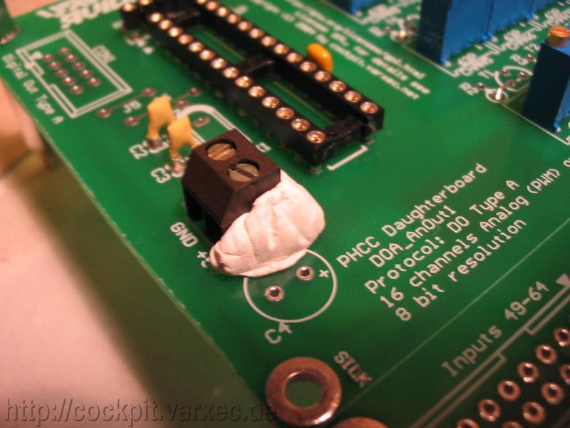 |
While held in place be the same method as used before, solder the screw clamp. |
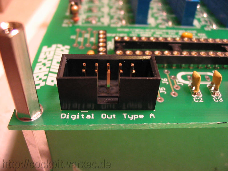 |
Moving on to CON1, pinheader that will provide connection to the PHCC motherboard... This one didn't need fixing since the holes were small and could hold the IDC connector used in place without help. Make sure that pin 1 and the cutout are pointing away from the board. |
|
|
Same thing with CON3, the connector for the 16 outputs. Again, pin 1 points away from the board. |
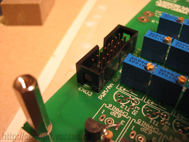 |
Solder CON1 and CON3. Soldering boards with solder mask is definatelty more fun than without. |
 |
C4, a 100uF (micro Farads) electrolytic capacitor, is next. Any voltage rating works, as we are just running 5V on this board and the lowest common voltage rating of electrolytics is 16V. |
 |
Finish the board by adding our last part, X1, the 10MHz crystal oscillator. Both HC18 and HC49 packages are ok. |
|
|
The finished board, ready for the PIC microcontroller. |
 |
Another view. |
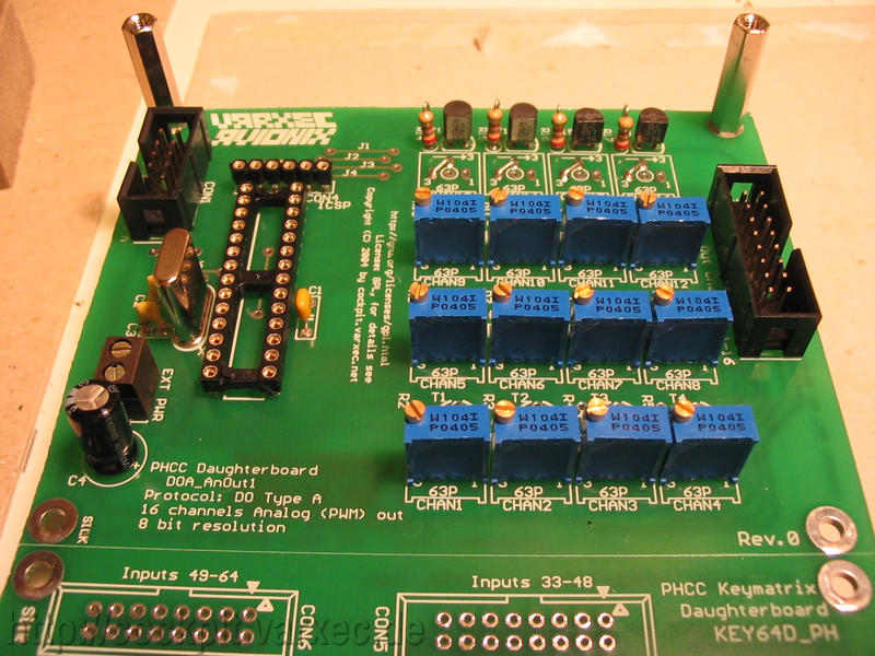 |
And yet another. |
Thats it :)